

10
M. P. Echlin et al.
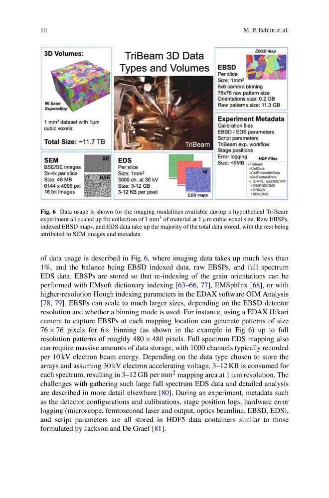
Fig. 6 Data usage is shown for the imaging modalities available during a hypothetical TriBeam
experiment all scaled up for collection of 1 mm 3 of material at 1 μm cubic voxel size. Raw EBSPs,
indexed EBSD maps, and EDS data take up the majority of the total data stored, with the rest being
attributed to SEM images and metadata
of data usage is described in Fig. 6, where imaging data takes up much less than
1%, and the balance being EBSD indexed data, raw EBSPs, and full spectrum
EDS data. EBSPs are stored so that re-indexing of the grain orientations can be
performed with EMsoft dictionary indexing [63–66, 77], EMSphInx [68], or with
higher-resolution Hough indexing parameters in the EDAX software OIM Analysis
[78, 79]. EBSPs can scale to much larger sizes, depending on the EBSD detector
resolution and whether a binning mode is used. For instance, using a EDAX Hikari
camera to capture EBSPs at each mapping location can generate patterns of size
76 × 76 pixels for 6× binning (as shown in the example in Fig. 6) up to full
resolution patterns of roughly 480 × 480 pixels. Full spectrum EDS mapping also
can require massive amounts of data storage, with 1000 channels typically recorded
per 10 kV electron beam energy. Depending on the data type chosen to store the
arrays and assuming 30 kV electron accelerating voltage, 3–12 KB is consumed for
each spectrum, resulting in 3–12 GB per mm 2 mapping area at 1 μm resolution. The
challenges with gathering such large full spectrum EDS data and detailed analysis
are described in more detail elsewhere [80]. During an experiment, metadata such
as the detector configurations and calibrations, stage position logs, hardware error
logging (microscope, femtosecond laser and output, optics beamline, EBSD, EDS),
and script parameters are all stored in HDF5 data containers similar to those
formulated by Jackson and De Graef [81].
M. P. Echlin et al.
Fig. 6 Data usage is shown for the imaging modalities available during a hypothetical TriBeam
experiment all scaled up for collection of 1 mm 3 of material at 1 μm cubic voxel size. Raw EBSPs,
indexed EBSD maps, and EDS data take up the majority of the total data stored, with the rest being
attributed to SEM images and metadata
of data usage is described in Fig. 6, where imaging data takes up much less than
1%, and the balance being EBSD indexed data, raw EBSPs, and full spectrum
EDS data. EBSPs are stored so that re-indexing of the grain orientations can be
performed with EMsoft dictionary indexing [63–66, 77], EMSphInx [68], or with
higher-resolution Hough indexing parameters in the EDAX software OIM Analysis
[78, 79]. EBSPs can scale to much larger sizes, depending on the EBSD detector
resolution and whether a binning mode is used. For instance, using a EDAX Hikari
camera to capture EBSPs at each mapping location can generate patterns of size
76 × 76 pixels for 6× binning (as shown in the example in Fig. 6) up to full
resolution patterns of roughly 480 × 480 pixels. Full spectrum EDS mapping also
can require massive amounts of data storage, with 1000 channels typically recorded
per 10 kV electron beam energy. Depending on the data type chosen to store the
arrays and assuming 30 kV electron accelerating voltage, 3–12 KB is consumed for
each spectrum, resulting in 3–12 GB per mm 2 mapping area at 1 μm resolution. The
challenges with gathering such large full spectrum EDS data and detailed analysis
are described in more detail elsewhere [80]. During an experiment, metadata such
as the detector configurations and calibrations, stage position logs, hardware error
logging (microscope, femtosecond laser and output, optics beamline, EBSD, EDS),
and script parameters are all stored in HDF5 data containers similar to those
formulated by Jackson and De Graef [81].