

38
Compact Models for Integrated Circuit Design
and are related to the respective mobility by the relationship [6]
D
D
kT
q
v
n
n
p
p
kT
µ
µ
=
=
≡
(2.42)
where:
v
kT q
kT ≡
is called the thermal voltage
Equation 2.42 is often referred to as the Einstein’s relation. For lightly
doped silicon (e.g., N d ≅ 1 × 10 15 cm –3 ) at room temperature, D n = 38 cm 2
sec –1 and D p = 13 cm 2 sec –1 . The negative sign in Equation 2.41 implies that
the hole current flows in a direction opposite to the hole concentration
gradient.
2.2.5.6 Nonuniformly Doped Semiconductors and Built-In Electric Field
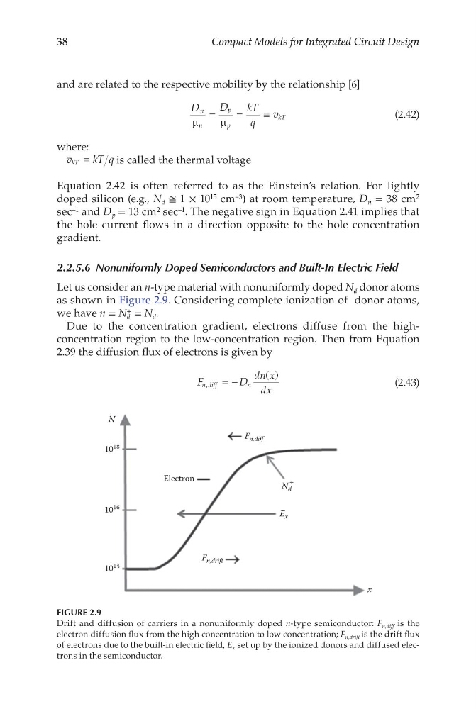
Let us consider an n-type material with nonuniformly doped N d donor atoms
as shown in Figure 2.9. Considering complete ionization of donor atoms,
we have n = N d
+ = N d .
Due to the concentration gradient, electrons diffuse from the highconcentration region to the low-concentration region. Then from Equation
2.39 the diffusion flux of electrons is given by
F
D
dn x
dx
n diff
n
,
( )
= −
(2.43)
10 14
F n,drift
F n,diff
E x
x
10 16
10
18
Electron
N
N d
+
FIGURE 2.9
Drift and diffusion of carriers in a nonuniformly doped n-type semiconductor: F n,diff is the
electron diffusion flux from the high concentration to low concentration; F n,drift is the drift flux
of electrons due to the built-in electric field, E x set up by the ionized donors and diffused electrons in the semiconductor.
Compact Models for Integrated Circuit Design
and are related to the respective mobility by the relationship [6]
D
D
kT
q
v
n
n
p
p
kT
µ
µ
=
=
≡
(2.42)
where:
v
kT q
kT ≡
is called the thermal voltage
Equation 2.42 is often referred to as the Einstein’s relation. For lightly
doped silicon (e.g., N d ≅ 1 × 10 15 cm –3 ) at room temperature, D n = 38 cm 2
sec –1 and D p = 13 cm 2 sec –1 . The negative sign in Equation 2.41 implies that
the hole current flows in a direction opposite to the hole concentration
gradient.
2.2.5.6 Nonuniformly Doped Semiconductors and Built-In Electric Field
Let us consider an n-type material with nonuniformly doped N d donor atoms
as shown in Figure 2.9. Considering complete ionization of donor atoms,
we have n = N d
+ = N d .
Due to the concentration gradient, electrons diffuse from the highconcentration region to the low-concentration region. Then from Equation
2.39 the diffusion flux of electrons is given by
F
D
dn x
dx
n diff
n
,
( )
= −
(2.43)
10 14
F n,drift
F n,diff
E x
x
10 16
10
18
Electron
N
N d
+
FIGURE 2.9
Drift and diffusion of carriers in a nonuniformly doped n-type semiconductor: F n,diff is the
electron diffusion flux from the high concentration to low concentration; F n,drift is the drift flux
of electrons due to the built-in electric field, E x set up by the ionized donors and diffused electrons in the semiconductor.