

28
Compact Models for Integrated Circuit Design
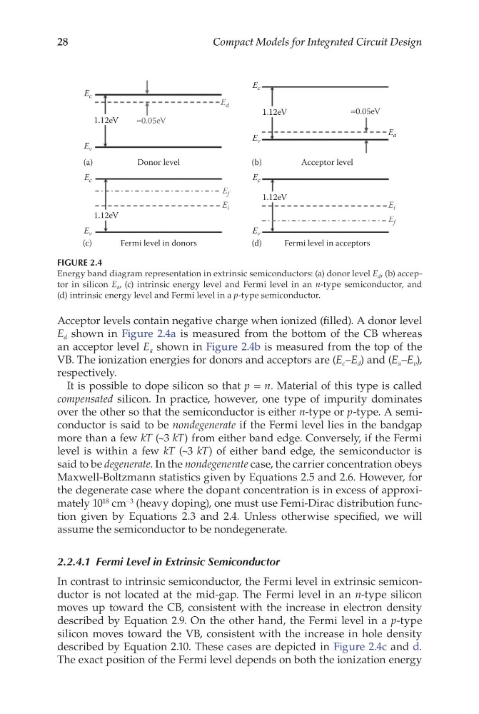
Acceptor levels contain negative charge when ionized (filled). A donor level
E d shown in Figure 2.4a is measured from the bottom of the CB whereas
an acceptor level E a shown in Figure 2.4b is measured from the top of the
VB. The ionization energies for donors and acceptors are (E c –E d ) and (E a –E v ),
respectively.
It is possible to dope silicon so that p = n. Material of this type is called
compensated silicon. In practice, however, one type of impurity dominates
over the other so that the semiconductor is either n-type or p-type. A semiconductor is said to be nondegenerate if the Fermi level lies in the bandgap
more than a few kT (~3 kT) from either band edge. Conversely, if the Fermi
level is within a few kT (~3 kT) of either band edge, the semiconductor is
said to be degenerate. In the nondegenerate case, the carrier concentration obeys
Maxwell-Boltzmann statistics given by Equations 2.5 and 2.6. However, for
the degenerate case where the dopant concentration is in excess of approximately 10 18 cm –3 (heavy doping), one must use Femi-Dirac distribution function given by Equations 2.3 and 2.4. Unless otherwise specified, we will
assume the semiconductor to be nondegenerate.
2.2.4.1 Fermi Level in Extrinsic Semiconductor
In contrast to intrinsic semiconductor, the Fermi level in extrinsic semiconductor is not located at the mid-gap. The Fermi level in an n-type silicon
moves up toward the CB, consistent with the increase in electron density
described by Equation 2.9. On the other hand, the Fermi level in a p-type
silicon moves toward the VB, consistent with the increase in hole density
described by Equation 2.10. These cases are depicted in Figure 2.4c and d.
The exact position of the Fermi level depends on both the ionization energy
Donor level
Fermi level in donors
E c
1.12eV
E d
≈0.05eV
E v
1.12eV
E f
E i
E c
E v
Acceptor level
Fermi level in acceptors
E c
1.12eV
≈0.05eV
E v
1.12eV
E i
E f
E c
E v
(a)
(c)
(d)
(b)
E a
FIGURE 2.4
Energy band diagram representation in extrinsic semiconductors: (a) donor level E d , (b) acceptor in silicon E a , (c) intrinsic energy level and Fermi level in an n-type semiconductor, and
(d) intrinsic energy level and Fermi level in a p-type semiconductor.
Compact Models for Integrated Circuit Design
Acceptor levels contain negative charge when ionized (filled). A donor level
E d shown in Figure 2.4a is measured from the bottom of the CB whereas
an acceptor level E a shown in Figure 2.4b is measured from the top of the
VB. The ionization energies for donors and acceptors are (E c –E d ) and (E a –E v ),
respectively.
It is possible to dope silicon so that p = n. Material of this type is called
compensated silicon. In practice, however, one type of impurity dominates
over the other so that the semiconductor is either n-type or p-type. A semiconductor is said to be nondegenerate if the Fermi level lies in the bandgap
more than a few kT (~3 kT) from either band edge. Conversely, if the Fermi
level is within a few kT (~3 kT) of either band edge, the semiconductor is
said to be degenerate. In the nondegenerate case, the carrier concentration obeys
Maxwell-Boltzmann statistics given by Equations 2.5 and 2.6. However, for
the degenerate case where the dopant concentration is in excess of approximately 10 18 cm –3 (heavy doping), one must use Femi-Dirac distribution function given by Equations 2.3 and 2.4. Unless otherwise specified, we will
assume the semiconductor to be nondegenerate.
2.2.4.1 Fermi Level in Extrinsic Semiconductor
In contrast to intrinsic semiconductor, the Fermi level in extrinsic semiconductor is not located at the mid-gap. The Fermi level in an n-type silicon
moves up toward the CB, consistent with the increase in electron density
described by Equation 2.9. On the other hand, the Fermi level in a p-type
silicon moves toward the VB, consistent with the increase in hole density
described by Equation 2.10. These cases are depicted in Figure 2.4c and d.
The exact position of the Fermi level depends on both the ionization energy
Donor level
Fermi level in donors
E c
1.12eV
E d
≈0.05eV
E v
1.12eV
E f
E i
E c
E v
Acceptor level
Fermi level in acceptors
E c
1.12eV
≈0.05eV
E v
1.12eV
E i
E f
E c
E v
(a)
(c)
(d)
(b)
E a
FIGURE 2.4
Energy band diagram representation in extrinsic semiconductors: (a) donor level E d , (b) acceptor in silicon E a , (c) intrinsic energy level and Fermi level in an n-type semiconductor, and
(d) intrinsic energy level and Fermi level in a p-type semiconductor.