

26
Compact Models for Integrated Circuit Design
due to the charged atomic cores of the host atoms in a regular lattice, giving
rise to a periodic potential energy. The effect of the periodic potential of the
crystal lattice on the motion of electrons in the CB and holes in the VB is represented by the effective masses of the electrons (m n
* ) and holes (m p
* ), respectively. In practice, there are several types of mass used for a given material
and carrier type [1–11]. The effective mass required to calculate the carrier
(electron and hole) concentration is called the density of states effective mass,
whereas the mass required to calculate carrier mobility is called the conductivity effective mass. These effective masses depend on temperature. There is a
large variation in the reported values of m n
* and m p
* [16]. The commonly used
values for the effective mass for electrons and holes at room temperature are
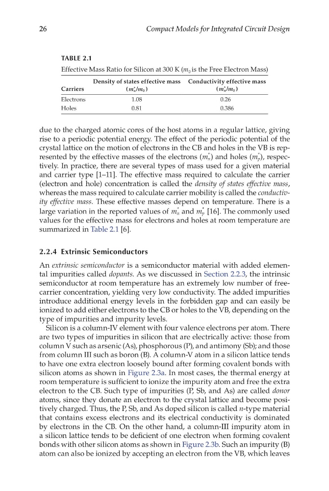
summarized in Table 2.1 [6].
2.2.4 Extrinsic Semiconductors
An extrinsic semiconductor is a semiconductor material with added elemental impurities called dopants. As we discussed in Section 2.2.3, the intrinsic
semiconductor at room temperature has an extremely low number of freecarrier concentration, yielding very low conductivity. The added impurities
introduce additional energy levels in the forbidden gap and can easily be
ionized to add either electrons to the CB or holes to the VB, depending on the
type of impurities and impurity levels.
Silicon is a column-IV element with four valence electrons per atom. There
are two types of impurities in silicon that are electrically active: those from
column V such as arsenic (As), phosphorous (P), and antimony (Sb); and those
from column III such as boron (B). A column-V atom in a silicon lattice tends
to have one extra electron loosely bound after forming covalent bonds with
silicon atoms as shown in Figure 2.3a. In most cases, the thermal energy at
room temperature is sufficient to ionize the impurity atom and free the extra
electron to the CB. Such type of impurities (P, Sb, and As) are called donor
atoms, since they donate an electron to the crystal lattice and become positively charged. Thus, the P, Sb, and As doped silicon is called n-type material
that contains excess electrons and its electrical conductivity is dominated
by electrons in the CB. On the other hand, a column-III impurity atom in
a silicon lattice tends to be deficient of one electron when forming covalent
bonds with other silicon atoms as shown in Figure 2.3b. Such an impurity (B)
atom can also be ionized by accepting an electron from the VB, which leaves
TABLE 2.1
Effective Mass Ratio for Silicon at 300 K (m 0 is the Free Electron Mass)
Carriers
Density of states effective mass
(
)
m m
n
* / 0
Conductivity effective mass
(
)
m m
n
*
0
/
Electrons
1.08
0.26
Holes
0.81
0.386
Compact Models for Integrated Circuit Design
due to the charged atomic cores of the host atoms in a regular lattice, giving
rise to a periodic potential energy. The effect of the periodic potential of the
crystal lattice on the motion of electrons in the CB and holes in the VB is represented by the effective masses of the electrons (m n
* ) and holes (m p
* ), respectively. In practice, there are several types of mass used for a given material
and carrier type [1–11]. The effective mass required to calculate the carrier
(electron and hole) concentration is called the density of states effective mass,
whereas the mass required to calculate carrier mobility is called the conductivity effective mass. These effective masses depend on temperature. There is a
large variation in the reported values of m n
* and m p
* [16]. The commonly used
values for the effective mass for electrons and holes at room temperature are
summarized in Table 2.1 [6].
2.2.4 Extrinsic Semiconductors
An extrinsic semiconductor is a semiconductor material with added elemental impurities called dopants. As we discussed in Section 2.2.3, the intrinsic
semiconductor at room temperature has an extremely low number of freecarrier concentration, yielding very low conductivity. The added impurities
introduce additional energy levels in the forbidden gap and can easily be
ionized to add either electrons to the CB or holes to the VB, depending on the
type of impurities and impurity levels.
Silicon is a column-IV element with four valence electrons per atom. There
are two types of impurities in silicon that are electrically active: those from
column V such as arsenic (As), phosphorous (P), and antimony (Sb); and those
from column III such as boron (B). A column-V atom in a silicon lattice tends
to have one extra electron loosely bound after forming covalent bonds with
silicon atoms as shown in Figure 2.3a. In most cases, the thermal energy at
room temperature is sufficient to ionize the impurity atom and free the extra
electron to the CB. Such type of impurities (P, Sb, and As) are called donor
atoms, since they donate an electron to the crystal lattice and become positively charged. Thus, the P, Sb, and As doped silicon is called n-type material
that contains excess electrons and its electrical conductivity is dominated
by electrons in the CB. On the other hand, a column-III impurity atom in
a silicon lattice tends to be deficient of one electron when forming covalent
bonds with other silicon atoms as shown in Figure 2.3b. Such an impurity (B)
atom can also be ionized by accepting an electron from the VB, which leaves
TABLE 2.1
Effective Mass Ratio for Silicon at 300 K (m 0 is the Free Electron Mass)
Carriers
Density of states effective mass
(
)
m m
n
* / 0
Conductivity effective mass
(
)
m m
n
*
0
/
Electrons
1.08
0.26
Holes
0.81
0.386