

390
Compact Models for Integrated Circuit Design
forward transit time of the carriers to reach from the emitter to collector, then the total minority carrier charge due to forward current
I CC is given by
Q
Q Q
Q Q
I
I
DE
E
B E
B
BC
E
E B
B
CB CC
Fdc CC
=
+
+
+
=
+
+ +
=
(
)
τ τ
τ τ
τ
(11.39)
where:
τ Fdc is the total forward delay time consisting of emitter delay τ E
EB space charge layer transit time τ EB
base transit time τ B
CB-space charge layer transit time τ CB
From Equation 11.39, we can write the expression for the diffusion
capacitance C DE (V BE ) due to the applied bias V BE
C V
Q
V
I
V
DE
DE
B E
Fdc CC
B E
BE
( )=
=
′ ′
′ ′
τ
(11.40)
The base transit time τ B is the major contributor of total transistor
delay time τ Fdc given in Equation 11.39. Thus, τ B is the most critical
parameter to determine the speed of BJTs. In the absence of built-in
electric fields in the base (i.e., constant N a ) with low-level injection,
the injected electron concentration n p varies linearly across the base
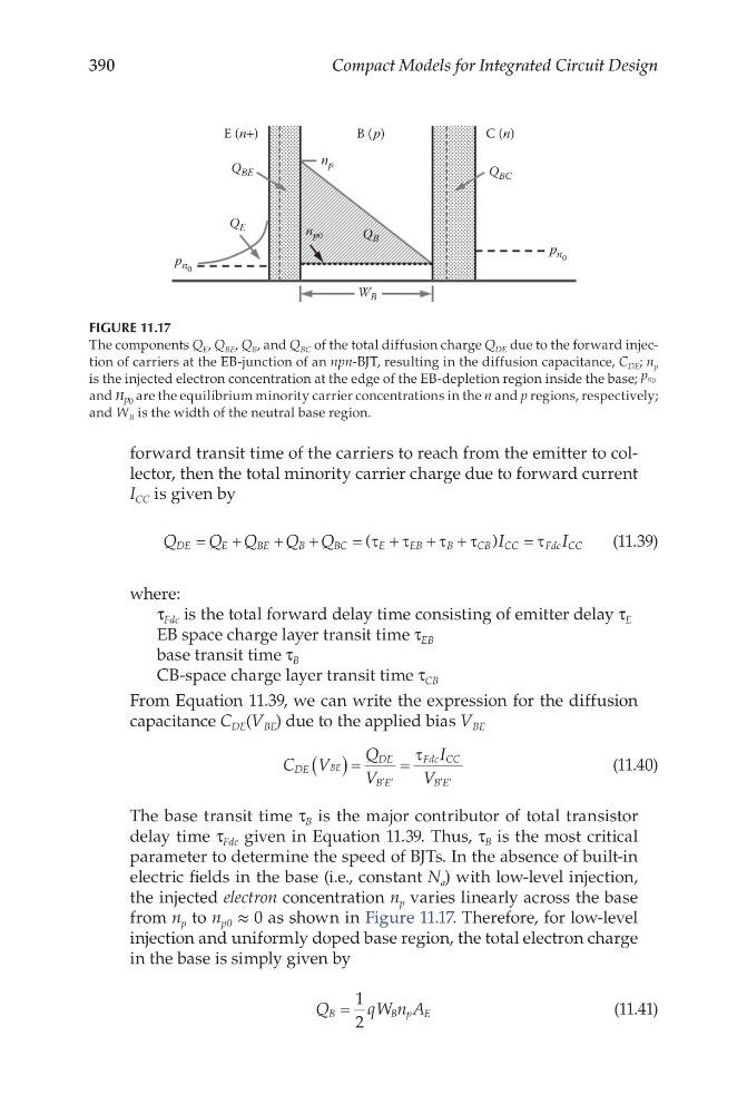
from n p to n p0 ≈ 0 as shown in Figure 11.17. Therefore, for low-level
injection and uniformly doped base region, the total electron charge
in the base is simply given by
Q
qW n A
B
Bp E
=
1
2
(11.41)
C (n)
B (p)
E (n+)
W B
Q BE
Q BC
Q E
Q B
n p
n p0
p n 0
p n 0
FIGURE 11.17
The components Q E , Q BE , Q B , and Q BC of the total diffusion charge Q DE due to the forward injection of carriers at the EB-junction of an npn-BJT, resulting in the diffusion capacitance, C DE ; n p
is the injected electron concentration at the edge of the EB-depletion region inside the base; p n0
and n p0 are the equilibrium minority carrier concentrations in the n and p regions, respectively;
and W B is the width of the neutral base region.
Compact Models for Integrated Circuit Design
forward transit time of the carriers to reach from the emitter to collector, then the total minority carrier charge due to forward current
I CC is given by
Q
Q Q
Q Q
I
I
DE
E
B E
B
BC
E
E B
B
CB CC
Fdc CC
=
+
+
+
=
+
+ +
=
(
)
τ τ
τ τ
τ
(11.39)
where:
τ Fdc is the total forward delay time consisting of emitter delay τ E
EB space charge layer transit time τ EB
base transit time τ B
CB-space charge layer transit time τ CB
From Equation 11.39, we can write the expression for the diffusion
capacitance C DE (V BE ) due to the applied bias V BE
C V
Q
V
I
V
DE
DE
B E
Fdc CC
B E
BE
( )=
=
′ ′
′ ′
τ
(11.40)
The base transit time τ B is the major contributor of total transistor
delay time τ Fdc given in Equation 11.39. Thus, τ B is the most critical
parameter to determine the speed of BJTs. In the absence of built-in
electric fields in the base (i.e., constant N a ) with low-level injection,
the injected electron concentration n p varies linearly across the base
from n p to n p0 ≈ 0 as shown in Figure 11.17. Therefore, for low-level
injection and uniformly doped base region, the total electron charge
in the base is simply given by
Q
qW n A
B
Bp E
=
1
2
(11.41)
C (n)
B (p)
E (n+)
W B
Q BE
Q BC
Q E
Q B
n p
n p0
p n 0
p n 0
FIGURE 11.17
The components Q E , Q BE , Q B , and Q BC of the total diffusion charge Q DE due to the forward injection of carriers at the EB-junction of an npn-BJT, resulting in the diffusion capacitance, C DE ; n p
is the injected electron concentration at the edge of the EB-depletion region inside the base; p n0
and n p0 are the equilibrium minority carrier concentrations in the n and p regions, respectively;
and W B is the width of the neutral base region.