

388
Compact Models for Integrated Circuit Design
• Effect of emitter series resistance, r e : The ohmic drop due to r e reduces
the EB-junction potential V BE by a factor of r e I E by the emitter current
I E so that
∆V
I r
I I r I
r
BE
E e
C
B e
B
F e
=
=
+
(
) =
+
(
)
1 β
(11.34)
From Equation 11.34 we find that r e results in an equivalent base
resistance of (1 + β F )r e . Since the emitter region is heavily doped
(≥1 × 10 19 cm −3 ), r e is negligibly small. However, due to the contact resistance at the emitter terminal and since β F >> 1, a typical
value of r e is about 5 ohm is obtained. Therefore, though the value
of r e is very small, it affects both I C and I B due to the voltage drop
∆V
I
r
BE
B
F e
=
+
(
)
1 β
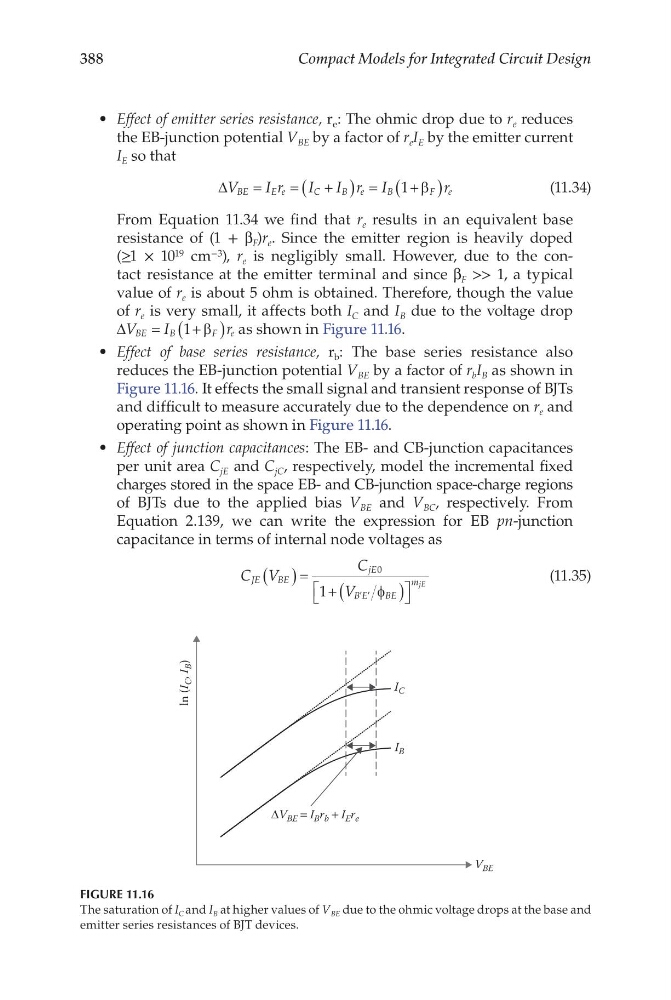
as shown in Figure 11.16.
• Effect of base series resistance, r b : The base series resistance also
reduces the EB-junction potential V BE by a factor of r b I B as shown in
Figure 11.16. It effects the small signal and transient response of BJTs
and difficult to measure accurately due to the dependence on r e and
operating point as shown in Figure 11.16.
• Effect of junction capacitances: The EB- and CB-junction capacitances
per unit area C jE and C jC , respectively, model the incremental fixed
charges stored in the space EB- and CB-junction space-charge regions
of BJTs due to the applied bias V BE and V BC , respectively. From
Equation 2.139, we can write the expression for EB pn-junction
capacitance in terms of internal node voltages as
C V
C
V
JE
BE
jE
B E
BE
mjE
( )= + (
)
′ ′
0
1
φ
(11.35)
ln (I
C , I
B )
I B
V BE
ΔV BE = I B r b + I E r e
I C
FIGURE 11.16
The saturation of I C and I B at higher values of V BE due to the ohmic voltage drops at the base and
emitter series resistances of BJT devices.
Compact Models for Integrated Circuit Design
• Effect of emitter series resistance, r e : The ohmic drop due to r e reduces
the EB-junction potential V BE by a factor of r e I E by the emitter current
I E so that
∆V
I r
I I r I
r
BE
E e
C
B e
B
F e
=
=
+
(
) =
+
(
)
1 β
(11.34)
From Equation 11.34 we find that r e results in an equivalent base
resistance of (1 + β F )r e . Since the emitter region is heavily doped
(≥1 × 10 19 cm −3 ), r e is negligibly small. However, due to the contact resistance at the emitter terminal and since β F >> 1, a typical
value of r e is about 5 ohm is obtained. Therefore, though the value
of r e is very small, it affects both I C and I B due to the voltage drop
∆V
I
r
BE
B
F e
=
+
(
)
1 β
as shown in Figure 11.16.
• Effect of base series resistance, r b : The base series resistance also
reduces the EB-junction potential V BE by a factor of r b I B as shown in
Figure 11.16. It effects the small signal and transient response of BJTs
and difficult to measure accurately due to the dependence on r e and
operating point as shown in Figure 11.16.
• Effect of junction capacitances: The EB- and CB-junction capacitances
per unit area C jE and C jC , respectively, model the incremental fixed
charges stored in the space EB- and CB-junction space-charge regions
of BJTs due to the applied bias V BE and V BC , respectively. From
Equation 2.139, we can write the expression for EB pn-junction
capacitance in terms of internal node voltages as
C V
C
V
JE
BE
jE
B E
BE
mjE
( )= + (
)
′ ′
0
1
φ
(11.35)
ln (I
C , I
B )
I B
V BE
ΔV BE = I B r b + I E r e
I C
FIGURE 11.16
The saturation of I C and I B at higher values of V BE due to the ohmic voltage drops at the base and
emitter series resistances of BJT devices.