

226
Compact Models for Integrated Circuit Design
6.2 Basic MOSFET Capacitance Model
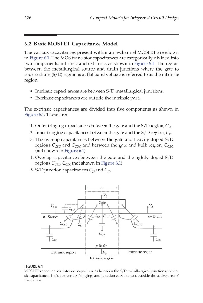
The various capacitances present within an n-channel MOSFET are shown
in Figure 6.1. The MOS transistor capacitances are categorically divided into
two components: intrinsic and extrinsic, as shown in Figure 6.1. The region
between the metallurgical source and drain junctions where the gate to
source-drain (S/D) region is at flat band voltage is referred to as the intrinsic
region.
• Intrinsic capacitances are between S/D metallurgical junctions.
• Extrinsic capacitances are outside the intrinsic part.
The extrinsic capacitances are divided into five components as shown in
Figure 6.1. These are:
1. Outer fringing capacitances between the gate and the S/D region, C FO
2. Inner fringing capacitances between the gate and the S/D region, C FI
3. The overlap capacitances between the gate and heavily doped S/D
regions C GSO and C GDO and between the gate and bulk region, C GBO
(not shown in Figure 6.1)
4. Overlap capacitances between the gate and the lightly doped S/D
regions C GSL , C GDL (not shown in Figure 6.1)
5. S/D junction capacitances C JS and C JD
L
Gate
Extrinsic region
Intrinsic region
Extrinsic region
V g
V s
V d
C FO
C GSO
C JS
C FI
C GB
C JD
C GDO
C GD
C GS
V b
p-Body
n+ Source
n+ Drain
FIGURE 6.1
MOSFET capacitances: intrinsic capacitances between the S/D metallurgical junctions; extrinsic capacitances include overlap, fringing, and junction capacitances outside the active area of
the device.
Compact Models for Integrated Circuit Design
6.2 Basic MOSFET Capacitance Model
The various capacitances present within an n-channel MOSFET are shown
in Figure 6.1. The MOS transistor capacitances are categorically divided into
two components: intrinsic and extrinsic, as shown in Figure 6.1. The region
between the metallurgical source and drain junctions where the gate to
source-drain (S/D) region is at flat band voltage is referred to as the intrinsic
region.
• Intrinsic capacitances are between S/D metallurgical junctions.
• Extrinsic capacitances are outside the intrinsic part.
The extrinsic capacitances are divided into five components as shown in
Figure 6.1. These are:
1. Outer fringing capacitances between the gate and the S/D region, C FO
2. Inner fringing capacitances between the gate and the S/D region, C FI
3. The overlap capacitances between the gate and heavily doped S/D
regions C GSO and C GDO and between the gate and bulk region, C GBO
(not shown in Figure 6.1)
4. Overlap capacitances between the gate and the lightly doped S/D
regions C GSL , C GDL (not shown in Figure 6.1)
5. S/D junction capacitances C JS and C JD
L
Gate
Extrinsic region
Intrinsic region
Extrinsic region
V g
V s
V d
C FO
C GSO
C JS
C FI
C GB
C JD
C GDO
C GD
C GS
V b
p-Body
n+ Source
n+ Drain
FIGURE 6.1
MOSFET capacitances: intrinsic capacitances between the S/D metallurgical junctions; extrinsic capacitances include overlap, fringing, and junction capacitances outside the active area of
the device.