

211
Compact Models for Small Geometry MOSFETs
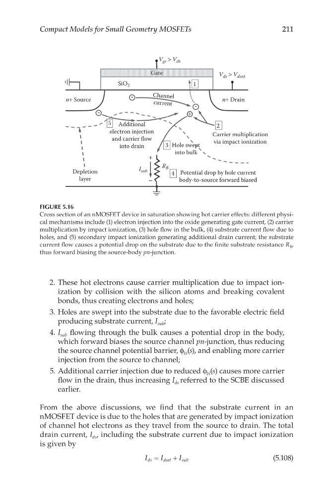
2. These hot electrons cause carrier multiplication due to impact ionization by collision with the silicon atoms and breaking covalent
bonds, thus creating electrons and holes;
3. Holes are swept into the substrate due to the favorable electric field
producing substrate current, I sub ;
4. I sub flowing through the bulk causes a potential drop in the body,
which forward biases the source channel pn-junction, thus reducing
the source channel potential barrier, f bi (s), and enabling more carrier
injection from the source to channel;
5. Additional carrier injection due to reduced f bi (s) causes more carrier
flow in the drain, thus increasing I ds referred to the SCBE discussed
earlier.
From the above discussions, we find that the substrate current in an
nMOSFET device is due to the holes that are generated by impact ionization
of channel hot electrons as they travel from the source to drain. The total
drain current, I ds , including the substrate current due to impact ionization
is given by
I
I
I
ds
dsat
sub
=
+
(5.108)
Depletion
layer
I sub
Additional
electron injection
and carrier flow
into drain
SiO 2
5
Gate
1
2
V ds > V dsat
V gs > V th
3
4
Hole swept
into bulk
Potential drop by hole current
body-to-source forward biased
Carrier multiplication
via impact ionization
n+ Drain
+
−
n+ Source
Cha nnel
curr ent
R B
FIGURE 5.16
Cross section of an nMOSFET device in saturation showing hot carrier effects: different physical mechanisms include (1) electron injection into the oxide generating gate current, (2) carrier
multiplication by impact ionization, (3) hole flow in the bulk, (4) substrate current flow due to
holes, and (5) secondary impact ionization generating additional drain current; the substrate
current flow causes a potential drop on the substrate due to the finite substrate resistance R B ,
thus forward biasing the source-body pn-junction.
Compact Models for Small Geometry MOSFETs
2. These hot electrons cause carrier multiplication due to impact ionization by collision with the silicon atoms and breaking covalent
bonds, thus creating electrons and holes;
3. Holes are swept into the substrate due to the favorable electric field
producing substrate current, I sub ;
4. I sub flowing through the bulk causes a potential drop in the body,
which forward biases the source channel pn-junction, thus reducing
the source channel potential barrier, f bi (s), and enabling more carrier
injection from the source to channel;
5. Additional carrier injection due to reduced f bi (s) causes more carrier
flow in the drain, thus increasing I ds referred to the SCBE discussed
earlier.
From the above discussions, we find that the substrate current in an
nMOSFET device is due to the holes that are generated by impact ionization
of channel hot electrons as they travel from the source to drain. The total
drain current, I ds , including the substrate current due to impact ionization
is given by
I
I
I
ds
dsat
sub
=
+
(5.108)
Depletion
layer
I sub
Additional
electron injection
and carrier flow
into drain
SiO 2
5
Gate
1
2
V ds > V dsat
V gs > V th
3
4
Hole swept
into bulk
Potential drop by hole current
body-to-source forward biased
Carrier multiplication
via impact ionization
n+ Drain
+
−
n+ Source
Cha nnel
curr ent
R B
FIGURE 5.16
Cross section of an nMOSFET device in saturation showing hot carrier effects: different physical mechanisms include (1) electron injection into the oxide generating gate current, (2) carrier
multiplication by impact ionization, (3) hole flow in the bulk, (4) substrate current flow due to
holes, and (5) secondary impact ionization generating additional drain current; the substrate
current flow causes a potential drop on the substrate due to the finite substrate resistance R B ,
thus forward biasing the source-body pn-junction.