

208
Compact Models for Integrated Circuit Design
V
V
a
a
a V
a V
aV
gseff
f b
s
fb
s
f b
s
gs
=
+
(
) − +
+
(
) −
(
) −
+
(
) +
=
φ
φ
φ
1
2
1
2
2
1
4
4
2
2
2
V V
a
a
a V
a V
a V
aV
fb
s
fb
s
f b
s
fb
s
g
+ −
+
+
(
) −
+
(
) + −
+
(
) +
φ
φ
φ
φ
1
2
1
2
4
4
1 4
4
2
2
2
2
s s
fb
s
f b
s
gs
fb
s
g s
f b
V
a
a
a V
aV
V
a
a V V
=
+ −
+
−
+
(
) +
=
+ +
+
−
−
φ
φ
φ
1
2
1
2
1 4
4
1
2
1 4
φ φ s
(
) −
(
)
1
(5.101)
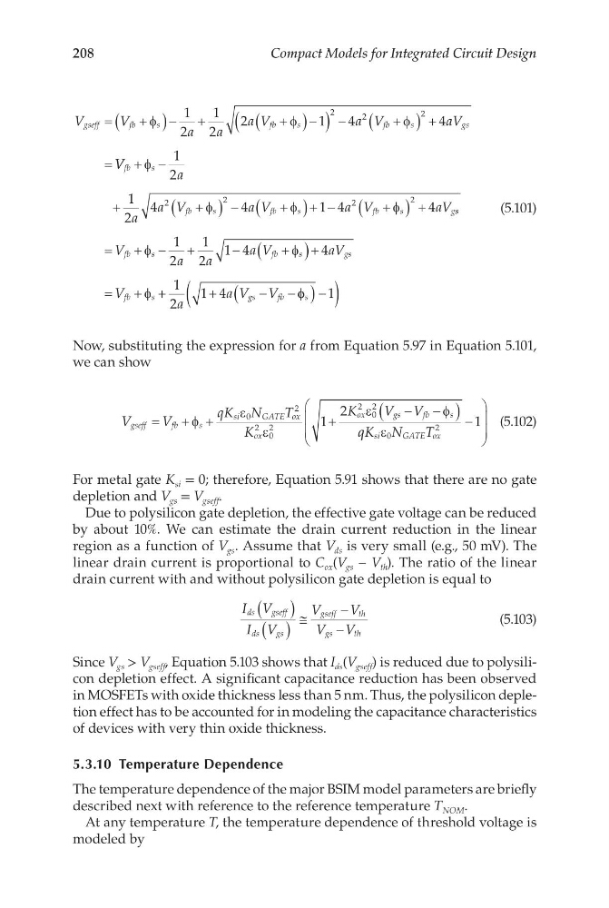
Now, substituting the expression for a from Equation 5.97 in Equation 5.101,
we can show
V
V
qK N
T
K
K
V V
gseff
f b
s
si
GATE ox
ox
ox
gs
fb
s
=
+ +
+
−
−
(
)
φ
ε
ε
ε
φ
0
2
2
0
2
2
0
2
1
2
q qK N
T
si
GATE ox
ε 0
2
1
−
(5.102)
For metal gate K si = 0; therefore, Equation 5.91 shows that there are no gate
depletion and V gs = V gseff .
Due to polysilicon gate depletion, the effective gate voltage can be reduced
by about 10%. We can estimate the drain current reduction in the linear
region as a function of V gs . Assume that V ds is very small (e.g., 50 mV). The
linear drain current is proportional to C ox (V gs − V th ). The ratio of the linear
drain current with and without polysilicon gate depletion is equal to
I V
I V
V
V
V V
ds
gseff
ds
gs
gseff
t h
gs
th
( )
( )
≅
−
−
(5.103)
Since V gs > V gseff , Equation 5.103 shows that I ds (V gseff ) is reduced due to polysilicon depletion effect. A significant capacitance reduction has been observed
in MOSFETs with oxide thickness less than 5 nm. Thus, the polysilicon depletion effect has to be accounted for in modeling the capacitance characteristics
of devices with very thin oxide thickness.
5.3.10 Temperature Dependence
The temperature dependence of the major BSIM model parameters are briefly
described next with reference to the reference temperature T NOM .
At any temperature T, the temperature dependence of threshold voltage is
modeled by
Compact Models for Integrated Circuit Design
V
V
a
a
a V
a V
aV
gseff
f b
s
fb
s
f b
s
gs
=
+
(
) − +
+
(
) −
(
) −
+
(
) +
=
φ
φ
φ
1
2
1
2
2
1
4
4
2
2
2
V V
a
a
a V
a V
a V
aV
fb
s
fb
s
f b
s
fb
s
g
+ −
+
+
(
) −
+
(
) + −
+
(
) +
φ
φ
φ
φ
1
2
1
2
4
4
1 4
4
2
2
2
2
s s
fb
s
f b
s
gs
fb
s
g s
f b
V
a
a
a V
aV
V
a
a V V
=
+ −
+
−
+
(
) +
=
+ +
+
−
−
φ
φ
φ
1
2
1
2
1 4
4
1
2
1 4
φ φ s
(
) −
(
)
1
(5.101)
Now, substituting the expression for a from Equation 5.97 in Equation 5.101,
we can show
V
V
qK N
T
K
K
V V
gseff
f b
s
si
GATE ox
ox
ox
gs
fb
s
=
+ +
+
−
−
(
)
φ
ε
ε
ε
φ
0
2
2
0
2
2
0
2
1
2
q qK N
T
si
GATE ox
ε 0
2
1
−
(5.102)
For metal gate K si = 0; therefore, Equation 5.91 shows that there are no gate
depletion and V gs = V gseff .
Due to polysilicon gate depletion, the effective gate voltage can be reduced
by about 10%. We can estimate the drain current reduction in the linear
region as a function of V gs . Assume that V ds is very small (e.g., 50 mV). The
linear drain current is proportional to C ox (V gs − V th ). The ratio of the linear
drain current with and without polysilicon gate depletion is equal to
I V
I V
V
V
V V
ds
gseff
ds
gs
gseff
t h
gs
th
( )
( )
≅
−
−
(5.103)
Since V gs > V gseff , Equation 5.103 shows that I ds (V gseff ) is reduced due to polysilicon depletion effect. A significant capacitance reduction has been observed
in MOSFETs with oxide thickness less than 5 nm. Thus, the polysilicon depletion effect has to be accounted for in modeling the capacitance characteristics
of devices with very thin oxide thickness.
5.3.10 Temperature Dependence
The temperature dependence of the major BSIM model parameters are briefly
described next with reference to the reference temperature T NOM .
At any temperature T, the temperature dependence of threshold voltage is
modeled by