

202
Compact Models for Integrated Circuit Design
bulk-charge effect as discussed in Chapter 4, defining the parameter called,
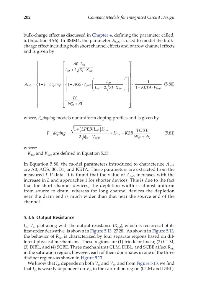
α (Equation 4.96). In BSIM4, the parameter A bulk is used to model the bulkcharge effect including both short channel effects and narrow channel effects
and is given by
A
F doping
A L
L
X J X
AGS V
L
L
bulk
eff
eff
d ep
gsteff
eff
ef
= +
⋅
⋅
+
⋅
⋅ −
⋅
1
0
2
1
_
f f
d ep
eff
XJ X
B
W
B
+
⋅
+ ′ +
2
0
1
2
⋅ +
⋅
1
1 KETA V bseff
(5.80)
where, F_doping models nonuniform doping profiles and is given by
F doping
LPEB L K
V
K
K B
TOXE
W
W
eff
o x
s
b seff
ox
eff
_
=
+ (
)
−
+
−
′ +
1
2
3
1
1
0
φ
(5.81)
where:
K 1ox and K 2ox are defined in Equation 5.35
In Equation 5.80, the model parameters introduced to characterize A bulk
are A0, AGS, B0, B1, and KETA. These parameters are extracted from the
measured I–V data. It is found that the value of A bulk increases with the
increase in L and approaches 1 for shorter devices. This is due to the fact
that for short channel devices, the depletion width is almost uniform
from source to drain, whereas for long channel devices the depletion
near the drain end is much wider than that near the source end of the
channel.
5.3.6 Output Resistance
I ds –V ds plot along with the output resistance (R out ), which is reciprocal of its
first-order derivative, is shown in Figure 5.13 [27,28]. As shown in Figure 5.13,
the behavior of R out is characterized by four separate regions based on different physical mechanisms. These regions are (1) triode or linear, (2) CLM,
(3) DIBL, and (4) SCBE. Three mechanisms CLM, DIBL, and SCBE affect R out
in the saturation region; however, each of them dominates in one of the three
distinct regions as shown in Figure 5.13.
We know that I ds depends on both V gs and V ds , and from Figure 5.13, we find
that I ds is weakly dependent on V ds in the saturation region (CLM and DIBL).
Compact Models for Integrated Circuit Design
bulk-charge effect as discussed in Chapter 4, defining the parameter called,
α (Equation 4.96). In BSIM4, the parameter A bulk is used to model the bulkcharge effect including both short channel effects and narrow channel effects
and is given by
A
F doping
A L
L
X J X
AGS V
L
L
bulk
eff
eff
d ep
gsteff
eff
ef
= +
⋅
⋅
+
⋅
⋅ −
⋅
1
0
2
1
_
f f
d ep
eff
XJ X
B
W
B
+
⋅
+ ′ +
2
0
1
2
⋅ +
⋅
1
1 KETA V bseff
(5.80)
where, F_doping models nonuniform doping profiles and is given by
F doping
LPEB L K
V
K
K B
TOXE
W
W
eff
o x
s
b seff
ox
eff
_
=
+ (
)
−
+
−
′ +
1
2
3
1
1
0
φ
(5.81)
where:
K 1ox and K 2ox are defined in Equation 5.35
In Equation 5.80, the model parameters introduced to characterize A bulk
are A0, AGS, B0, B1, and KETA. These parameters are extracted from the
measured I–V data. It is found that the value of A bulk increases with the
increase in L and approaches 1 for shorter devices. This is due to the fact
that for short channel devices, the depletion width is almost uniform
from source to drain, whereas for long channel devices the depletion
near the drain end is much wider than that near the source end of the
channel.
5.3.6 Output Resistance
I ds –V ds plot along with the output resistance (R out ), which is reciprocal of its
first-order derivative, is shown in Figure 5.13 [27,28]. As shown in Figure 5.13,
the behavior of R out is characterized by four separate regions based on different physical mechanisms. These regions are (1) triode or linear, (2) CLM,
(3) DIBL, and (4) SCBE. Three mechanisms CLM, DIBL, and SCBE affect R out
in the saturation region; however, each of them dominates in one of the three
distinct regions as shown in Figure 5.13.
We know that I ds depends on both V gs and V ds , and from Figure 5.13, we find
that I ds is weakly dependent on V ds in the saturation region (CLM and DIBL).