

158
Compact Models for Integrated Circuit Design
I
C
W
L
l L
V V
V V
C
V V
ds
s ox
d
gs
th
ds
dsat
s ox
g s
t
=
− ( )
−
(
)
>
=
−
µ
µ
2 1
2 ;
W
2L
h h
d
gs
th
d
l L
V V
l
L
(
) − ( )
=
−
(
) −
−
2
2
1
1
1
2
1
.
.
β
(4.84)
Using Equation 4.82 in Equation 4.84, we can show for V ds > V dsat
I
I
l
L
ds
dsat
d
=
−
−
1
1
(4.85)
In general, l d << L; therefore, by series expansion we get, 1
1
1
− ( )
≅ +(
)
−
l L
l L
d
d
.
Since l d increases with the increase of V ds , that is, l L
d
is directly proportional
to V ds , we can write 1
1
+ ( )= +
l L
V
d
d s
λ . Then Equation 4.85 becomes
I
I
V
ds
dsat
ds
=
+
(
)
1 λ
(4.86)
where:
λ is called the CLM parameter describing the effect of V ds on l d to model
CLM
0
0.0
0.2
0.4
0.6
Drain current (mA)
0.8
1.0
I ds @ V gs = 2 V
I ds @ V gs = 3 V
I ds @ V gs = 4 V
I ds @ V gs = 5 V
V dsat = V gs − V th
1
2
3
Drain voltage (V)
4
5
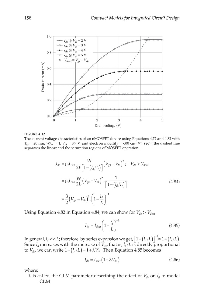
FIGURE 4.12
The current voltage characteristics of an nMOSFET device using Equations 4.72 and 4.82 with
T ox = 20 nm, W/L = 1, V th = 0.7 V, and electron mobility = 600 cm 2 V −1 sec −1 ; the dashed line
separates the linear and the saturation regions of MOSFET operation.
Compact Models for Integrated Circuit Design
I
C
W
L
l L
V V
V V
C
V V
ds
s ox
d
gs
th
ds
dsat
s ox
g s
t
=
− ( )
−
(
)
>
=
−
µ
µ
2 1
2 ;
W
2L
h h
d
gs
th
d
l L
V V
l
L
(
) − ( )
=
−
(
) −
−
2
2
1
1
1
2
1
.
.
β
(4.84)
Using Equation 4.82 in Equation 4.84, we can show for V ds > V dsat
I
I
l
L
ds
dsat
d
=
−
−
1
1
(4.85)
In general, l d << L; therefore, by series expansion we get, 1
1
1
− ( )
≅ +(
)
−
l L
l L
d
d
.
Since l d increases with the increase of V ds , that is, l L
d
is directly proportional
to V ds , we can write 1
1
+ ( )= +
l L
V
d
d s
λ . Then Equation 4.85 becomes
I
I
V
ds
dsat
ds
=
+
(
)
1 λ
(4.86)
where:
λ is called the CLM parameter describing the effect of V ds on l d to model
CLM
0
0.0
0.2
0.4
0.6
Drain current (mA)
0.8
1.0
I ds @ V gs = 2 V
I ds @ V gs = 3 V
I ds @ V gs = 4 V
I ds @ V gs = 5 V
V dsat = V gs − V th
1
2
3
Drain voltage (V)
4
5
FIGURE 4.12
The current voltage characteristics of an nMOSFET device using Equations 4.72 and 4.82 with
T ox = 20 nm, W/L = 1, V th = 0.7 V, and electron mobility = 600 cm 2 V −1 sec −1 ; the dashed line
separates the linear and the saturation regions of MOSFET operation.