

142
Compact Models for Integrated Circuit Design
I y
W qn x y
x y y
dx
ds
n
n
( )
( , ) ( , )
= −
∂
∂
=
∝
∫
µ
φ
0
constant
(4.22)
where μ n in Equation 4.22 is the channel electron surface mobility for
nMOSFETs, often referred to as the surface mobility μ s in order to distinguish it from the bulk mobility deep into the substrate described
in Section 2.2.5.1. In the rest of the discussion, we will replace μ n by
μ s to emphasize that the inversion layer mobility we deal with for
MOSFET devices is the surface mobility.
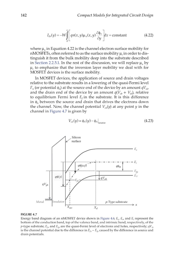
In MOSFET devices, the application of source and drain voltages
relative to the substrate results in a lowering of the quasi-Fermi level
F n (or potential f n ) at the source end of the device by an amount qV sb ,
and the drain end of the device by an amount q(V sb + V ds ), relative
to equilibrium Fermi level E f in the substrate. It is this difference
in f n between the source and drain that drives the electrons down
the channel. Now, the channel potential V ch (y) at any point y in the
channel in Figure 4.7 is given by
V y
y
ch
n
n
( )
( )
=
−
φ
φ source
(4.23)
Silicon
surface
p-Type substrate
x
X d
X inv
Insulator
Metal
qV gb
qV ch
qϕ(y)
qϕ B
qϕ(x,y)
E c
E i
E fp
E fn
E V
FIGURE 4.7
Energy band diagram of an nMOSFET device shown in Figure 4.6; E c , E v , and E i represent the
bottom of the conduction band, top of the valence band, and intrinsic band, respectively, of the
p-type substrate; E fn and E fp are the quasi-Fermi level of electrons and holes, respectively; qV ch
is the channel potential due to the difference in E fn − E fp caused by the difference in source and
drain potentials.
Compact Models for Integrated Circuit Design
I y
W qn x y
x y y
dx
ds
n
n
( )
( , ) ( , )
= −
∂
∂
=
∝
∫
µ
φ
0
constant
(4.22)
where μ n in Equation 4.22 is the channel electron surface mobility for
nMOSFETs, often referred to as the surface mobility μ s in order to distinguish it from the bulk mobility deep into the substrate described
in Section 2.2.5.1. In the rest of the discussion, we will replace μ n by
μ s to emphasize that the inversion layer mobility we deal with for
MOSFET devices is the surface mobility.
In MOSFET devices, the application of source and drain voltages
relative to the substrate results in a lowering of the quasi-Fermi level
F n (or potential f n ) at the source end of the device by an amount qV sb ,
and the drain end of the device by an amount q(V sb + V ds ), relative
to equilibrium Fermi level E f in the substrate. It is this difference
in f n between the source and drain that drives the electrons down
the channel. Now, the channel potential V ch (y) at any point y in the
channel in Figure 4.7 is given by
V y
y
ch
n
n
( )
( )
=
−
φ
φ source
(4.23)
Silicon
surface
p-Type substrate
x
X d
X inv
Insulator
Metal
qV gb
qV ch
qϕ(y)
qϕ B
qϕ(x,y)
E c
E i
E fp
E fn
E V
FIGURE 4.7
Energy band diagram of an nMOSFET device shown in Figure 4.6; E c , E v , and E i represent the
bottom of the conduction band, top of the valence band, and intrinsic band, respectively, of the
p-type substrate; E fn and E fp are the quasi-Fermi level of electrons and holes, respectively; qV ch
is the channel potential due to the difference in E fn − E fp caused by the difference in source and
drain potentials.