

140
Compact Models for Integrated Circuit Design
where:
n and p represent the electron and hole concentrations, respectively
q is the electronic charge
E is the electric field
f n and f p are the electron and hole quasi-Fermi potentials, respectively, in nonequilibrium condition
μ n and μ p are the electron and hole mobilities, respectively.
The total current density (J) flowing through the device is given by
J = J n + J p .
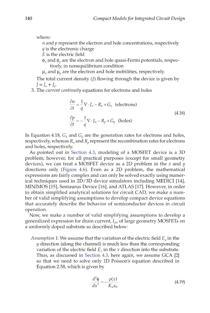
3. The current continuity equations for electrons and holes
∂
∂
= ∇
− +
∂
∂
= − ∇
− +
n
t q
J R G
p
t
q
J R G
n
n
n
n
p
p
1
1
⋅
⋅
(electrons)
holes)
(
(4.18)
In Equation 4.18, G n and G p are the generation rates for electrons and holes,
respectively, whereas R n and R p represent the recombination rates for electrons
and holes, respectively.
As pointed out in Section 4.3, modeling of a MOSFET device is a 3D
problem; however, for all practical purposes (except for small geometry
devices), we can treat a MOSFET device as a 2D problem in the x and y
directions only (Figure 4.6). Even as a 2D problem, the mathematical
expressions are fairly complex and can only be solved exactly using numerical techniques used in 2D/3D device simulators including MEDICI [14],
MINIMOS [15], Sentaurus Device [16], and ATLAS [17]. However, in order
to obtain simplified analytical solutions for circuit CAD, we make a number of valid simplifying assumptions to develop compact device equations
that accurately describe the behavior of semiconductor devices in circuit
operation.
Now, we make a number of valid simplifying assumptions to develop a
generalized expression for drain current, I ds , of large geometry MOSFETs on
a uniformly doped substrate as described below:
Assumption 1: We assume that the variation of the electric field E y in the
y direction (along the channel) is much less than the corresponding
variation of the electric field E x in the x direction into the substrate.
Thus, as discussed in Section 4.3, here again, we assume GCA [2]
so that we need to solve only 1D Poisson’s equation described in
Equation 2.58, which is given by
d
dx
x
K si
2
2
0
φ
ρ
ε
= −
( )
(4.19)
Compact Models for Integrated Circuit Design
where:
n and p represent the electron and hole concentrations, respectively
q is the electronic charge
E is the electric field
f n and f p are the electron and hole quasi-Fermi potentials, respectively, in nonequilibrium condition
μ n and μ p are the electron and hole mobilities, respectively.
The total current density (J) flowing through the device is given by
J = J n + J p .
3. The current continuity equations for electrons and holes
∂
∂
= ∇
− +
∂
∂
= − ∇
− +
n
t q
J R G
p
t
q
J R G
n
n
n
n
p
p
1
1
⋅
⋅
(electrons)
holes)
(
(4.18)
In Equation 4.18, G n and G p are the generation rates for electrons and holes,
respectively, whereas R n and R p represent the recombination rates for electrons
and holes, respectively.
As pointed out in Section 4.3, modeling of a MOSFET device is a 3D
problem; however, for all practical purposes (except for small geometry
devices), we can treat a MOSFET device as a 2D problem in the x and y
directions only (Figure 4.6). Even as a 2D problem, the mathematical
expressions are fairly complex and can only be solved exactly using numerical techniques used in 2D/3D device simulators including MEDICI [14],
MINIMOS [15], Sentaurus Device [16], and ATLAS [17]. However, in order
to obtain simplified analytical solutions for circuit CAD, we make a number of valid simplifying assumptions to develop compact device equations
that accurately describe the behavior of semiconductor devices in circuit
operation.
Now, we make a number of valid simplifying assumptions to develop a
generalized expression for drain current, I ds , of large geometry MOSFETs on
a uniformly doped substrate as described below:
Assumption 1: We assume that the variation of the electric field E y in the
y direction (along the channel) is much less than the corresponding
variation of the electric field E x in the x direction into the substrate.
Thus, as discussed in Section 4.3, here again, we assume GCA [2]
so that we need to solve only 1D Poisson’s equation described in
Equation 2.58, which is given by
d
dx
x
K si
2
2
0
φ
ρ
ε
= −
( )
(4.19)