

129
Metal-Oxide-Semiconductor System
b. Calculate and plot log(Q i ) versus surface potential f s for f s = 0.3
to 1.1. Clearly, label different operating regimes of the MOS capacitor system and explain.
c. Calculate and plot f s versus gate voltage V gs for V gs = 0 to 3.0 V.
Clearly label different operating regimes of the MOS capacitor
system and explain.
3.11 Consider an MOS capacitor system on a uniformly doped p-type
silicon substrate. In Section 3.4, MB probability distribution function
is used to solve Poisson’s equation in obtaining the surface charge Q s
in the semiconductor of the MOS capacitor system as a function of
surface potential. Use the same procedure as in Section 3.4 and FD
probability distribution function to obtain an expression similar to
Equation 3.52 for Q s as a function of surface potential in the semiconductor of the same MOS-capacitor system. Plot Q s versus surface
potential and compare with the plot in Figure 3.12.
p-Silicon
N a = 1 × 10
17 cm
−3
n-Silicon
N d = 1 × 10
17 cm
−3
Metal gate
V g
SiO 2
T ox
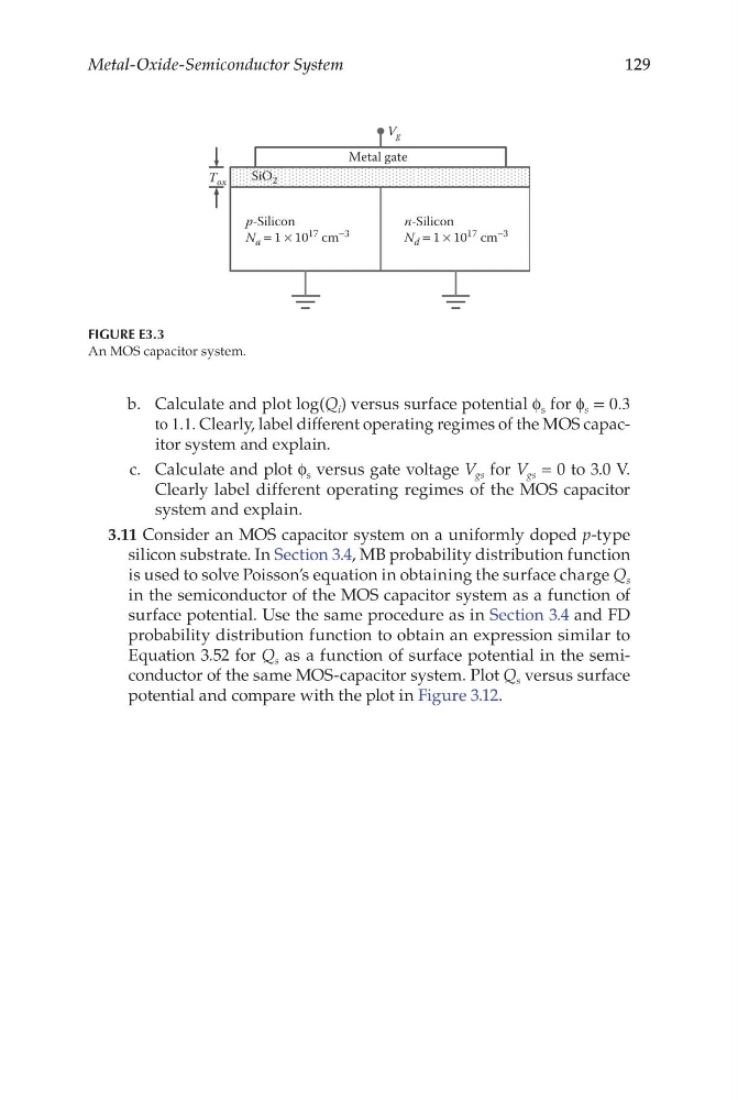
FIGURE E3.3
An MOS capacitor system.
Metal-Oxide-Semiconductor System
b. Calculate and plot log(Q i ) versus surface potential f s for f s = 0.3
to 1.1. Clearly, label different operating regimes of the MOS capacitor system and explain.
c. Calculate and plot f s versus gate voltage V gs for V gs = 0 to 3.0 V.
Clearly label different operating regimes of the MOS capacitor
system and explain.
3.11 Consider an MOS capacitor system on a uniformly doped p-type
silicon substrate. In Section 3.4, MB probability distribution function
is used to solve Poisson’s equation in obtaining the surface charge Q s
in the semiconductor of the MOS capacitor system as a function of
surface potential. Use the same procedure as in Section 3.4 and FD
probability distribution function to obtain an expression similar to
Equation 3.52 for Q s as a function of surface potential in the semiconductor of the same MOS-capacitor system. Plot Q s versus surface
potential and compare with the plot in Figure 3.12.
p-Silicon
N a = 1 × 10
17 cm
−3
n-Silicon
N d = 1 × 10
17 cm
−3
Metal gate
V g
SiO 2
T ox
FIGURE E3.3
An MOS capacitor system.