

115
Metal-Oxide-Semiconductor System
dV dV d
g
o x
s
=
+ φ
(3.85)
From Equations 3.84 and 3.85, we can show that
dV
d Q
dV
d Q
d
d Q
g
s
ox
s
s
s
(
)
(
)
(
)
−
= −
+ −
φ
∴
=
+
1
1
1
C C
C
ox
s
(3.86)
Thus, the total capacitance of an MOS structure equals the oxide capacitance
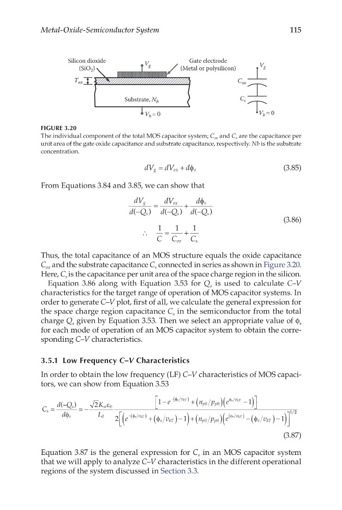
C ox and the substrate capacitance C s connected in series as shown in Figure 3.20.
Here, C s is the capacitance per unit area of the space charge region in the silicon.
Equation 3.86 along with Equation 3.53 for Q s is used to calculate C–V
characteristics for the target range of operation of MOS capacitor systems. In
order to generate C–V plot, first of all, we calculate the general expression for
the space charge region capacitance C s in the semiconductor from the total
charge Q s given by Equation 3.53. Then we select an appropriate value of f s
for each mode of operation of an MOS capacitor system to obtain the corresponding C–V characteristics.
3.5.1 Low Frequency C–V Characteristics
In order to obtain the low frequency (LF) C–V characteristics of MOS capacitors, we can show from Equation 3.53
C
d Q
d
K
L
e
n p
e
e
s
s
s
si
d
v
p
p
v
s kT
s kT
=
−
= −
−
+ (
)
−
(
)
−(
)
(
)
φ
ε
φ
φ
2
1
1
2
0
0
0
− −(
)
(
)
+ (
)−
(
) + (
)
− (
)−
(
)
φ
φ
φ
φ
s kT
s kT
v
s
k T
p
p
v
s
k T
v
n p
e
v
1
1
0
0
1/2 2
(3.87)
Equation 3.87 is the general expression for C s in an MOS capacitor system
that we will apply to analyze C–V characteristics in the different operational
regions of the system discussed in Section 3.3.
Silicon dioxide
(SiO 2 )
V g
V g
V b = 0
V b = 0
Gate electrode
(Metal or polysilicon)
Substrate, N b
T ox
C ox
C s
FIGURE 3.20
The individual component of the total MOS capacitor system; C ox and C s are the capacitance per
unit area of the gate oxide capacitance and substrate capacitance, respectively. Nb is the substrate
concentration.
Metal-Oxide-Semiconductor System
dV dV d
g
o x
s
=
+ φ
(3.85)
From Equations 3.84 and 3.85, we can show that
dV
d Q
dV
d Q
d
d Q
g
s
ox
s
s
s
(
)
(
)
(
)
−
= −
+ −
φ
∴
=
+
1
1
1
C C
C
ox
s
(3.86)
Thus, the total capacitance of an MOS structure equals the oxide capacitance
C ox and the substrate capacitance C s connected in series as shown in Figure 3.20.
Here, C s is the capacitance per unit area of the space charge region in the silicon.
Equation 3.86 along with Equation 3.53 for Q s is used to calculate C–V
characteristics for the target range of operation of MOS capacitor systems. In
order to generate C–V plot, first of all, we calculate the general expression for
the space charge region capacitance C s in the semiconductor from the total
charge Q s given by Equation 3.53. Then we select an appropriate value of f s
for each mode of operation of an MOS capacitor system to obtain the corresponding C–V characteristics.
3.5.1 Low Frequency C–V Characteristics
In order to obtain the low frequency (LF) C–V characteristics of MOS capacitors, we can show from Equation 3.53
C
d Q
d
K
L
e
n p
e
e
s
s
s
si
d
v
p
p
v
s kT
s kT
=
−
= −
−
+ (
)
−
(
)
−(
)
(
)
φ
ε
φ
φ
2
1
1
2
0
0
0
− −(
)
(
)
+ (
)−
(
) + (
)
− (
)−
(
)
φ
φ
φ
φ
s kT
s kT
v
s
k T
p
p
v
s
k T
v
n p
e
v
1
1
0
0
1/2 2
(3.87)
Equation 3.87 is the general expression for C s in an MOS capacitor system
that we will apply to analyze C–V characteristics in the different operational
regions of the system discussed in Section 3.3.
Silicon dioxide
(SiO 2 )
V g
V g
V b = 0
V b = 0
Gate electrode
(Metal or polysilicon)
Substrate, N b
T ox
C ox
C s
FIGURE 3.20
The individual component of the total MOS capacitor system; C ox and C s are the capacitance per
unit area of the gate oxide capacitance and substrate capacitance, respectively. Nb is the substrate
concentration.