

109
Metal-Oxide-Semiconductor System
weak and strong inversion regions is defined by f s = 2f B ; that is, the inversion carrier concentration becomes equal to that of the majority carrier at
the surface.
In order to distinguish the transition region between the weak and strong
inversions, the inversion regime is divided into three regions. The third
region that lies between the weak and strong inversion is called the moderate inversion region, which lies between 2f B and (2f B + 6v kT ) as shown in
Figure 3.16. According to this convention, the region beyond (2f B + 6v kT ) is
the strong inversion region [7].
From the general expression of Q i Equation 3.70, we can derive the regional
expressions for Q i at weak and strong inversions.
Weak inversion sets in when the band bending at the surface exceeds f B and
extends to 2f B , that is, f B < f s < 2f B . Within this region, the inversion charge
Q i is small compared to the depletion layer charge Q b , that is,
Q
Q
i
b
<<
(
)
weak inversion
(3.71)
For a small f s , Equation 3.70 can be simplified to obtain Q i at weak inversion as
Q
qK N v e
i
s i
a kT
v
s
B
kT
= −
(
)
−
(
)
2
0
2
2
ε
φ
φ
weak inversion
(3.72)
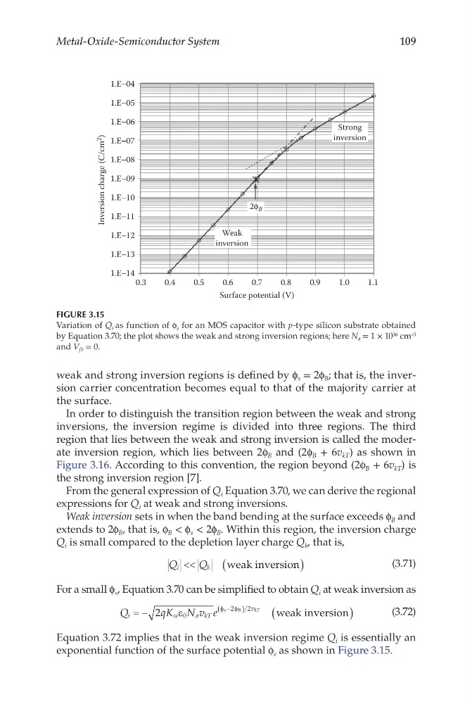
Equation 3.72 implies that in the weak inversion regime Q i is essentially an
exponential function of the surface potential f s as shown in Figure 3.15.
0.3
1.E−14
1.E−13
1.E−12
1.E−11
1.E−10
1.E−09
Inversion charge (C/cm
2
)
1.E−08
1.E−07
1.E−06
1.E−05
1.E−04
0.4
0.5
0.6
0.7
Surface potential (V)
0.8
0.9
1.0
1.1
Strong
inversion
2ϕ B
Weak
inversion
FIGURE 3.15
Variation of Q i as function of f s for an MOS capacitor with p-type silicon substrate obtained
by Equation 3.70; the plot shows the weak and strong inversion regions; here N a = 1 × 10 16 cm -3
and V fb = 0.
Metal-Oxide-Semiconductor System
weak and strong inversion regions is defined by f s = 2f B ; that is, the inversion carrier concentration becomes equal to that of the majority carrier at
the surface.
In order to distinguish the transition region between the weak and strong
inversions, the inversion regime is divided into three regions. The third
region that lies between the weak and strong inversion is called the moderate inversion region, which lies between 2f B and (2f B + 6v kT ) as shown in
Figure 3.16. According to this convention, the region beyond (2f B + 6v kT ) is
the strong inversion region [7].
From the general expression of Q i Equation 3.70, we can derive the regional
expressions for Q i at weak and strong inversions.
Weak inversion sets in when the band bending at the surface exceeds f B and
extends to 2f B , that is, f B < f s < 2f B . Within this region, the inversion charge
Q i is small compared to the depletion layer charge Q b , that is,
Q
Q
i
b
<<
(
)
weak inversion
(3.71)
For a small f s , Equation 3.70 can be simplified to obtain Q i at weak inversion as
Q
qK N v e
i
s i
a kT
v
s
B
kT
= −
(
)
−
(
)
2
0
2
2
ε
φ
φ
weak inversion
(3.72)
Equation 3.72 implies that in the weak inversion regime Q i is essentially an
exponential function of the surface potential f s as shown in Figure 3.15.
0.3
1.E−14
1.E−13
1.E−12
1.E−11
1.E−10
1.E−09
Inversion charge (C/cm
2
)
1.E−08
1.E−07
1.E−06
1.E−05
1.E−04
0.4
0.5
0.6
0.7
Surface potential (V)
0.8
0.9
1.0
1.1
Strong
inversion
2ϕ B
Weak
inversion
FIGURE 3.15
Variation of Q i as function of f s for an MOS capacitor with p-type silicon substrate obtained
by Equation 3.70; the plot shows the weak and strong inversion regions; here N a = 1 × 10 16 cm -3
and V fb = 0.