

Data Conversion Circuits – D/A and A/D Converters
501
-
+
Comp.
C 3
3V/4
-
+
C 2
V/2
-
+
Comp.
C 1
V/4
k
r
o
w
t
e
N
g
n i
d
o
C
s e
t
a
G
d
a
e
R
S
R
Q
S
R
Q
2
1
2
0
V A
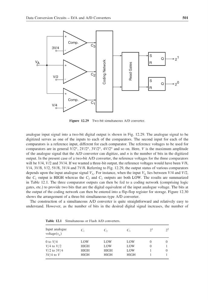
Figure 12.29 Two-bit simultaneous A/D converter.
analogue input signal into a two-bit digital output is shown in Fig. 12.29. The analogue signal to be
digitized serves as one of the inputs to each of the comparators. The second input for each of the
comparators is a reference input, different for each comparator. The reference voltages to be used for
comparators are in general V /2
n , 2V /2
n , 3V /2
n , 4V /2
n and so on. Here, V is the maximum amplitude
of the analogue signal that the A/D converter can digitize, and n is the number of bits in the digitized
output. In the present case of a two-bit A/D converter, the reference voltages for the three comparators
will be V /4, V /2 and 3V /4. If we wanted a three-bit output, the reference voltages would have been V /8,
V /4, 3V /8, V /2, 5V /8, 3V /4 and 7V /8. Referring to Fig. 12.29, the output status of various comparators
depends upon the input analogue signal V A . For instance, when the input V A lies between V /4 and V /2,
the C 1 output is HIGH whereas the C 2 and C 3 outputs are both LOW. The results are summarized
in Table 12.1. The three comparator outputs can then be fed to a coding network (comprising logic
gates, etc.) to provide two bits that are the digital equivalent of the input analogue voltage. The bits at
the output of the coding network can then be entered into a flip-flop register for storage. Figure 12.30
shows the arrangement of a three-bit simultaneous-type A/D converter.
The construction of a simultaneous A/D converter is quite straightforward and relatively easy to
understand. However, as the number of bits in the desired digital signal increases, the number of
Table 12.1 Simultaneous or Flash A/D converters.
Input analogue
voltagev a
C 1
C 2
C 3
2
1
2
2
0 to V/4
LOW
LOW
LOW
0
0
V/4 to V/2
HIGH
LOW
LOW
0
1
V/2 to 3V/4
HIGH
HIGH
LOW
1
0
3V/4 to V
HIGH
HIGH
HIGH
1
1
501
-
+
Comp.
C 3
3V/4
-
+
C 2
V/2
-
+
Comp.
C 1
V/4
k
r
o
w
t
e
N
g
n i
d
o
C
s e
t
a
G
d
a
e
R
S
R
Q
S
R
Q
2
1
2
0
V A
Figure 12.29 Two-bit simultaneous A/D converter.
analogue input signal into a two-bit digital output is shown in Fig. 12.29. The analogue signal to be
digitized serves as one of the inputs to each of the comparators. The second input for each of the
comparators is a reference input, different for each comparator. The reference voltages to be used for
comparators are in general V /2
n , 2V /2
n , 3V /2
n , 4V /2
n and so on. Here, V is the maximum amplitude
of the analogue signal that the A/D converter can digitize, and n is the number of bits in the digitized
output. In the present case of a two-bit A/D converter, the reference voltages for the three comparators
will be V /4, V /2 and 3V /4. If we wanted a three-bit output, the reference voltages would have been V /8,
V /4, 3V /8, V /2, 5V /8, 3V /4 and 7V /8. Referring to Fig. 12.29, the output status of various comparators
depends upon the input analogue signal V A . For instance, when the input V A lies between V /4 and V /2,
the C 1 output is HIGH whereas the C 2 and C 3 outputs are both LOW. The results are summarized
in Table 12.1. The three comparator outputs can then be fed to a coding network (comprising logic
gates, etc.) to provide two bits that are the digital equivalent of the input analogue voltage. The bits at
the output of the coding network can then be entered into a flip-flop register for storage. Figure 12.30
shows the arrangement of a three-bit simultaneous-type A/D converter.
The construction of a simultaneous A/D converter is quite straightforward and relatively easy to
understand. However, as the number of bits in the desired digital signal increases, the number of
Table 12.1 Simultaneous or Flash A/D converters.
Input analogue
voltagev a
C 1
C 2
C 3
2
1
2
2
0 to V/4
LOW
LOW
LOW
0
0
V/4 to V/2
HIGH
LOW
LOW
0
1
V/2 to 3V/4
HIGH
HIGH
LOW
1
0
3V/4 to V
HIGH
HIGH
HIGH
1
1