

Programmable Logic Devices
319
00
01
11
10
B1B0
00
01
11
10
A A
1 0
0
0
0
0
1
1
1
1
1
1
0
0
0
0
0
0
(d)
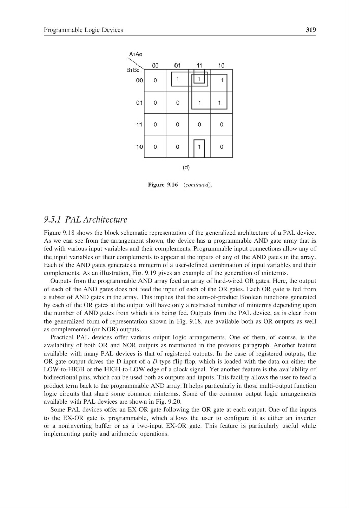
Figure 9.16 (continued).
9.5.1 PAL Architecture
Figure 9.18 shows the block schematic representation of the generalized architecture of a PAL device.
As we can see from the arrangement shown, the device has a programmable AND gate array that is
fed with various input variables and their complements. Programmable input connections allow any of
the input variables or their complements to appear at the inputs of any of the AND gates in the array.
Each of the AND gates generates a minterm of a user-defined combination of input variables and their
complements. As an illustration, Fig. 9.19 gives an example of the generation of minterms.
Outputs from the programmable AND array feed an array of hard-wired OR gates. Here, the output
of each of the AND gates does not feed the input of each of the OR gates. Each OR gate is fed from
a subset of AND gates in the array. This implies that the sum-of-product Boolean functions generated
by each of the OR gates at the output will have only a restricted number of minterms depending upon
the number of AND gates from which it is being fed. Outputs from the PAL device, as is clear from
the generalized form of representation shown in Fig. 9.18, are available both as OR outputs as well
as complemented (or NOR) outputs.
Practical PAL devices offer various output logic arrangements. One of them, of course, is the
availability of both OR and NOR outputs as mentioned in the previous paragraph. Another feature
available with many PAL devices is that of registered outputs. In the case of registered outputs, the
OR gate output drives the D-input of a D-type flip-flop, which is loaded with the data on either the
LOW-to-HIGH or the HIGH-to-LOW edge of a clock signal. Yet another feature is the availability of
bidirectional pins, which can be used both as outputs and inputs. This facility allows the user to feed a
product term back to the programmable AND array. It helps particularly in those multi-output function
logic circuits that share some common minterms. Some of the common output logic arrangements
available with PAL devices are shown in Fig. 9.20.
Some PAL devices offer an EX-OR gate following the OR gate at each output. One of the inputs
to the EX-OR gate is programmable, which allows the user to configure it as either an inverter
or a noninverting buffer or as a two-input EX-OR gate. This feature is particularly useful while
implementing parity and arithmetic operations.
319
00
01
11
10
B1B0
00
01
11
10
A A
1 0
0
0
0
0
1
1
1
1
1
1
0
0
0
0
0
0
(d)
Figure 9.16 (continued).
9.5.1 PAL Architecture
Figure 9.18 shows the block schematic representation of the generalized architecture of a PAL device.
As we can see from the arrangement shown, the device has a programmable AND gate array that is
fed with various input variables and their complements. Programmable input connections allow any of
the input variables or their complements to appear at the inputs of any of the AND gates in the array.
Each of the AND gates generates a minterm of a user-defined combination of input variables and their
complements. As an illustration, Fig. 9.19 gives an example of the generation of minterms.
Outputs from the programmable AND array feed an array of hard-wired OR gates. Here, the output
of each of the AND gates does not feed the input of each of the OR gates. Each OR gate is fed from
a subset of AND gates in the array. This implies that the sum-of-product Boolean functions generated
by each of the OR gates at the output will have only a restricted number of minterms depending upon
the number of AND gates from which it is being fed. Outputs from the PAL device, as is clear from
the generalized form of representation shown in Fig. 9.18, are available both as OR outputs as well
as complemented (or NOR) outputs.
Practical PAL devices offer various output logic arrangements. One of them, of course, is the
availability of both OR and NOR outputs as mentioned in the previous paragraph. Another feature
available with many PAL devices is that of registered outputs. In the case of registered outputs, the
OR gate output drives the D-input of a D-type flip-flop, which is loaded with the data on either the
LOW-to-HIGH or the HIGH-to-LOW edge of a clock signal. Yet another feature is the availability of
bidirectional pins, which can be used both as outputs and inputs. This facility allows the user to feed a
product term back to the programmable AND array. It helps particularly in those multi-output function
logic circuits that share some common minterms. Some of the common output logic arrangements
available with PAL devices are shown in Fig. 9.20.
Some PAL devices offer an EX-OR gate following the OR gate at each output. One of the inputs
to the EX-OR gate is programmable, which allows the user to configure it as either an inverter
or a noninverting buffer or as a two-input EX-OR gate. This feature is particularly useful while
implementing parity and arithmetic operations.