

300
Digital Electronics
logic functions. In terms of the internal schematic arrangement of the two types of device, the circuits
or building blocks and their interconnections in a fixed logic device are permanent and cannot be
altered after the device is manufactured.
A programmable logic device offers to the user a wide range of logic capacity in terms of digital
building blocks, which can be configured by the user to perform the intended function or set of functions.
This configuration can be modified or altered any number of times by the user by reprogramming the
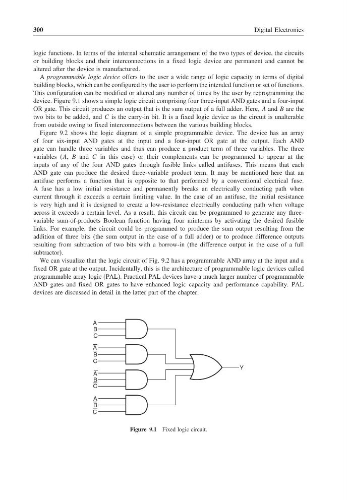
device. Figure 9.1 shows a simple logic circuit comprising four three-input AND gates and a four-input
OR gate. This circuit produces an output that is the sum output of a full adder. Here, A and B are the
two bits to be added, and C is the carry-in bit. It is a fixed logic device as the circuit is unalterable
from outside owing to fixed interconnections between the various building blocks.
Figure 9.2 shows the logic diagram of a simple programmable device. The device has an array
of four six-input AND gates at the input and a four-input OR gate at the output. Each AND
gate can handle three variables and thus can produce a product term of three variables. The three
variables (A, B and C in this case) or their complements can be programmed to appear at the
inputs of any of the four AND gates through fusible links called antifuses. This means that each
AND gate can produce the desired three-variable product term. It may be mentioned here that an
antifuse performs a function that is opposite to that performed by a conventional electrical fuse.
A fuse has a low initial resistance and permanently breaks an electrically conducting path when
current through it exceeds a certain limiting value. In the case of an antifuse, the initial resistance
is very high and it is designed to create a low-resistance electrically conducting path when voltage
across it exceeds a certain level. As a result, this circuit can be programmed to generate any threevariable sum-of-products Boolean function having four minterms by activating the desired fusible
links. For example, the circuit could be programmed to produce the sum output resulting from the
addition of three bits (the sum output in the case of a full adder) or to produce difference outputs
resulting from subtraction of two bits with a borrow-in (the difference output in the case of a full
subtractor).
We can visualize that the logic circuit of Fig. 9.2 has a programmable AND array at the input and a
fixed OR gate at the output. Incidentally, this is the architecture of programmable logic devices called
programmable array logic (PAL). Practical PAL devices have a much larger number of programmable
AND gates and fixed OR gates to have enhanced logic capacity and performance capability. PAL
devices are discussed in detail in the latter part of the chapter.
A
B
C
A
B
C
A
B
C
A
B
C
Y
Figure 9.1 Fixed logic circuit.
Digital Electronics
logic functions. In terms of the internal schematic arrangement of the two types of device, the circuits
or building blocks and their interconnections in a fixed logic device are permanent and cannot be
altered after the device is manufactured.
A programmable logic device offers to the user a wide range of logic capacity in terms of digital
building blocks, which can be configured by the user to perform the intended function or set of functions.
This configuration can be modified or altered any number of times by the user by reprogramming the
device. Figure 9.1 shows a simple logic circuit comprising four three-input AND gates and a four-input
OR gate. This circuit produces an output that is the sum output of a full adder. Here, A and B are the
two bits to be added, and C is the carry-in bit. It is a fixed logic device as the circuit is unalterable
from outside owing to fixed interconnections between the various building blocks.
Figure 9.2 shows the logic diagram of a simple programmable device. The device has an array
of four six-input AND gates at the input and a four-input OR gate at the output. Each AND
gate can handle three variables and thus can produce a product term of three variables. The three
variables (A, B and C in this case) or their complements can be programmed to appear at the
inputs of any of the four AND gates through fusible links called antifuses. This means that each
AND gate can produce the desired three-variable product term. It may be mentioned here that an
antifuse performs a function that is opposite to that performed by a conventional electrical fuse.
A fuse has a low initial resistance and permanently breaks an electrically conducting path when
current through it exceeds a certain limiting value. In the case of an antifuse, the initial resistance
is very high and it is designed to create a low-resistance electrically conducting path when voltage
across it exceeds a certain level. As a result, this circuit can be programmed to generate any threevariable sum-of-products Boolean function having four minterms by activating the desired fusible
links. For example, the circuit could be programmed to produce the sum output resulting from the
addition of three bits (the sum output in the case of a full adder) or to produce difference outputs
resulting from subtraction of two bits with a borrow-in (the difference output in the case of a full
subtractor).
We can visualize that the logic circuit of Fig. 9.2 has a programmable AND array at the input and a
fixed OR gate at the output. Incidentally, this is the architecture of programmable logic devices called
programmable array logic (PAL). Practical PAL devices have a much larger number of programmable
AND gates and fixed OR gates to have enhanced logic capacity and performance capability. PAL
devices are discussed in detail in the latter part of the chapter.
A
B
C
A
B
C
A
B
C
A
B
C
Y
Figure 9.1 Fixed logic circuit.