

Logic Families
163
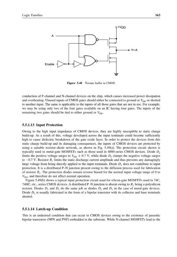
Figure 5.48 Tristate buffer in CMOS.
conduction of P-channel and N-channel devices on the chip, which causes increased power dissipation
and overheating. Unused inputs of CMOS gates should either be connected to ground or V DD or shorted
to another input. The same is applicable to the inputs of all those gates that are not in use. For example,
we may be using only two of the four gates available on an IC having four gates. The inputs of the
remaining two gates should be tied to either ground or V DD .
5.5.1.13 Input Protection
Owing to the high input impedance of CMOS devices, they are highly susceptible to static charge
build-up. As a result of this, voltage developed across the input terminals could become sufficiently
high to cause dielectric breakdown of the gate oxide layer. In order to protect the devices from this
static charge build-up and its damaging consequences, the inputs of CMOS devices are protected by
using a suitable resistor–diode network, as shown in Fig. 5.49(a). The protection circuit shown is
typically used in metal-gate MOSFETs such as those used in 4000-series CMOS devices. Diode D 2
limits the positive voltage surges to V DD + 0.7 V, while diode D 3 clamps the negative voltage surges
to −0.7 V. Resistor R 1 limits the static discharge current amplitude and thus prevents any damagingly
large voltage from being directly applied to the input terminals. Diode D 1 does not contribute to input
protection. It is a distributed P–N junction present owing to the diffusion process used for fabrication
of resistor R 1 . The protection diodes remain reverse biased for the normal input voltage range of 0 to
V DD , and therefore do not affect normal operation.
Figure 5.49(b) shows a typical input protection circuit used for silicon-gate MOSFETs used in 74C,
74HC, etc., series CMOS devices. A distributed P–N junction is absent owing to R 1 being a polysilicon
resistor. Diodes D 1 and D 2 do the same job as diodes D 2 and D 3 in the case of metal-gate devices.
Diode D 2 is usually fabricated in the form of a bipolar transistor with its collector and base terminals
shorted.
5.5.1.14 Latch-up Condition
This is an undesired condition that can occur in CMOS devices owing to the existence of parasitic
bipolar transistors (NPN and PNP) embedded in the substrate. While N-channel MOSFETs lead to the
163
Figure 5.48 Tristate buffer in CMOS.
conduction of P-channel and N-channel devices on the chip, which causes increased power dissipation
and overheating. Unused inputs of CMOS gates should either be connected to ground or V DD or shorted
to another input. The same is applicable to the inputs of all those gates that are not in use. For example,
we may be using only two of the four gates available on an IC having four gates. The inputs of the
remaining two gates should be tied to either ground or V DD .
5.5.1.13 Input Protection
Owing to the high input impedance of CMOS devices, they are highly susceptible to static charge
build-up. As a result of this, voltage developed across the input terminals could become sufficiently
high to cause dielectric breakdown of the gate oxide layer. In order to protect the devices from this
static charge build-up and its damaging consequences, the inputs of CMOS devices are protected by
using a suitable resistor–diode network, as shown in Fig. 5.49(a). The protection circuit shown is
typically used in metal-gate MOSFETs such as those used in 4000-series CMOS devices. Diode D 2
limits the positive voltage surges to V DD + 0.7 V, while diode D 3 clamps the negative voltage surges
to −0.7 V. Resistor R 1 limits the static discharge current amplitude and thus prevents any damagingly
large voltage from being directly applied to the input terminals. Diode D 1 does not contribute to input
protection. It is a distributed P–N junction present owing to the diffusion process used for fabrication
of resistor R 1 . The protection diodes remain reverse biased for the normal input voltage range of 0 to
V DD , and therefore do not affect normal operation.
Figure 5.49(b) shows a typical input protection circuit used for silicon-gate MOSFETs used in 74C,
74HC, etc., series CMOS devices. A distributed P–N junction is absent owing to R 1 being a polysilicon
resistor. Diodes D 1 and D 2 do the same job as diodes D 2 and D 3 in the case of metal-gate devices.
Diode D 2 is usually fabricated in the form of a bipolar transistor with its collector and base terminals
shorted.
5.5.1.14 Latch-up Condition
This is an undesired condition that can occur in CMOS devices owing to the existence of parasitic
bipolar transistors (NPN and PNP) embedded in the substrate. While N-channel MOSFETs lead to the