

98
Digital Electronics
The output of an inverter belonging to this family feeds the clock inputs of various flip-flops belonging
to the same family. How many flip-flops can be driven by the output of this inverter providing the clock
signal? Incidentally, the data given above are taken from the data sheet of a Schottky TTL family.
Solution
• The HIGH-state fan-out = 1/005 = 20 and the LOW-state fan-out = 20/2 = 10.
• Since the lower of the two fan-out values is 10, the inverter output can drive a maximum of 10
flip-flops.
4.11 Buffers and Transceivers
Logic gates, discussed in the previous pages, have a limited load-driving capability. A buffer has a
larger load-driving capability than a logic gate. It could be an inverting or noninverting buffer with a
single input, a NAND buffer, a NOR buffer, an OR buffer or an AND buffer. ‘Driver’ is another name
for a buffer. A driver is sometimes used to designate a circuit that has even larger drive capability than
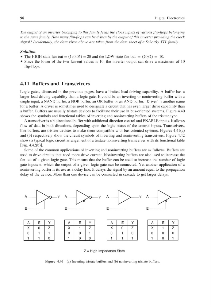
a buffer. Buffers are usually tristate devices to facilitate their use in bus-oriented systems. Figure 4.40
shows the symbols and functional tables of inverting and noninverting buffers of the tristate type.
A transceiver is a bidirectional buffer with additional direction control and ENABLE inputs. It allows
flow of data in both directions, depending upon the logic status of the control inputs. Transceivers,
like buffers, are tristate devices to make them compatible with bus-oriented systems. Figures 4.41(a)
and (b) respectively show the circuit symbols of inverting and noninverting transceivers. Figure 4.42
shows a typical logic circuit arrangement of a tristate noninverting transceiver with its functional table
[Fig. 4.42(b)].
Some of the common applications of inverting and noninverting buffers are as follows. Buffers are
used to drive circuits that need more drive current. Noninverting buffers are also used to increase the
fan-out of a given logic gate. This means that the buffer can be used to increase the number of logic
gate inputs to which the output of a given logic gate can be connected. Yet another application of a
noninverting buffer is its use as a delay line. It delays the signal by an amount equal to the propagation
delay of the device. More than one device can be connected in cascade to get larger delays.
A
E
Y A
E
Y
A
E
Y A
E
Y
A
X
0
1
E
0
1
1
Y
Z
1
0
A
X
0
1
E
1
0
0
Y
Z
1
0
A
X
0
1
E
0
1
1
Y
Z
0
1
A
X
0
1
E
1
0
0
Y
Z
0
1
Z = High Impedance State
Figure 4.40 (a) Inverting tristate buffers and (b) noninverting tristate buffers.
Digital Electronics
The output of an inverter belonging to this family feeds the clock inputs of various flip-flops belonging
to the same family. How many flip-flops can be driven by the output of this inverter providing the clock
signal? Incidentally, the data given above are taken from the data sheet of a Schottky TTL family.
Solution
• The HIGH-state fan-out = 1/005 = 20 and the LOW-state fan-out = 20/2 = 10.
• Since the lower of the two fan-out values is 10, the inverter output can drive a maximum of 10
flip-flops.
4.11 Buffers and Transceivers
Logic gates, discussed in the previous pages, have a limited load-driving capability. A buffer has a
larger load-driving capability than a logic gate. It could be an inverting or noninverting buffer with a
single input, a NAND buffer, a NOR buffer, an OR buffer or an AND buffer. ‘Driver’ is another name
for a buffer. A driver is sometimes used to designate a circuit that has even larger drive capability than
a buffer. Buffers are usually tristate devices to facilitate their use in bus-oriented systems. Figure 4.40
shows the symbols and functional tables of inverting and noninverting buffers of the tristate type.
A transceiver is a bidirectional buffer with additional direction control and ENABLE inputs. It allows
flow of data in both directions, depending upon the logic status of the control inputs. Transceivers,
like buffers, are tristate devices to make them compatible with bus-oriented systems. Figures 4.41(a)
and (b) respectively show the circuit symbols of inverting and noninverting transceivers. Figure 4.42
shows a typical logic circuit arrangement of a tristate noninverting transceiver with its functional table
[Fig. 4.42(b)].
Some of the common applications of inverting and noninverting buffers are as follows. Buffers are
used to drive circuits that need more drive current. Noninverting buffers are also used to increase the
fan-out of a given logic gate. This means that the buffer can be used to increase the number of logic
gate inputs to which the output of a given logic gate can be connected. Yet another application of a
noninverting buffer is its use as a delay line. It delays the signal by an amount equal to the propagation
delay of the device. More than one device can be connected in cascade to get larger delays.
A
E
Y A
E
Y
A
E
Y A
E
Y
A
X
0
1
E
0
1
1
Y
Z
1
0
A
X
0
1
E
1
0
0
Y
Z
1
0
A
X
0
1
E
0
1
1
Y
Z
0
1
A
X
0
1
E
1
0
0
Y
Z
0
1
Z = High Impedance State
Figure 4.40 (a) Inverting tristate buffers and (b) noninverting tristate buffers.