

Logic Gates and Related Devices
93
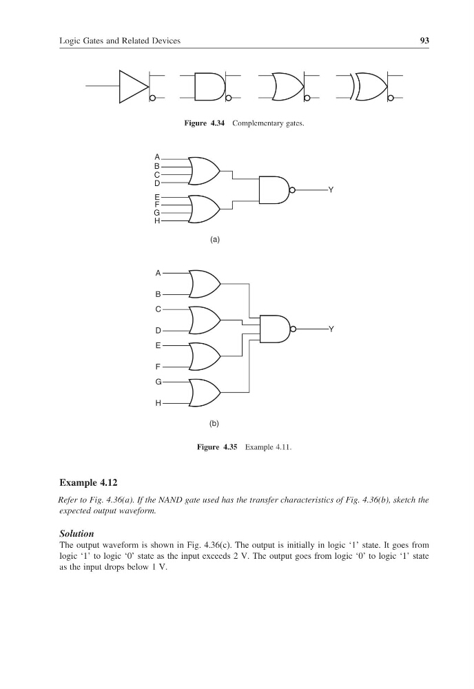
Figure 4.34 Complementary gates.
Y
A
B
D
C
E
F
H
G
(a)
A
B
C
D
E
F
G
H
Y
(b)
Figure 4.35 Example 4.11.
Example 4.12
Refer to Fig. 4.36(a). If the NAND gate used has the transfer characteristics of Fig. 4.36(b), sketch the
expected output waveform.
Solution
The output waveform is shown in Fig. 4.36(c). The output is initially in logic ‘1’ state. It goes from
logic ‘1’ to logic ‘0’ state as the input exceeds 2 V. The output goes from logic ‘0’ to logic ‘1’ state
as the input drops below 1 V.
93
Figure 4.34 Complementary gates.
Y
A
B
D
C
E
F
H
G
(a)
A
B
C
D
E
F
G
H
Y
(b)
Figure 4.35 Example 4.11.
Example 4.12
Refer to Fig. 4.36(a). If the NAND gate used has the transfer characteristics of Fig. 4.36(b), sketch the
expected output waveform.
Solution
The output waveform is shown in Fig. 4.36(c). The output is initially in logic ‘1’ state. It goes from
logic ‘1’ to logic ‘0’ state as the input exceeds 2 V. The output goes from logic ‘0’ to logic ‘1’ state
as the input drops below 1 V.