

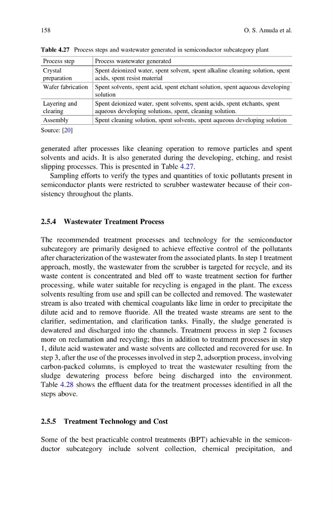
generated after processes like cleaning operation to remove particles and spent
solvents and acids. It is also generated during the developing, etching, and resist
slipping processes. This is presented in Table 4.27.
Sampling efforts to verify the types and quantities of toxic pollutants present in
semiconductor plants were restricted to scrubber wastewater because of their consistency throughout the plants.
2.5.4 Wastewater Treatment Process
The recommended treatment processes and technology for the semiconductor
subcategory are primarily designed to achieve effective control of the pollutants
after characterization of the wastewater from the associated plants. In step 1 treatment
approach, mostly, the wastewater from the scrubber is targeted for recycle, and its
waste content is concentrated and bled off to waste treatment section for further
processing, while water suitable for recycling is engaged in the plant. The excess
solvents resulting from use and spill can be collected and removed. The wastewater
stream is also treated with chemical coagulants like lime in order to precipitate the
dilute acid and to remove fluoride. All the treated waste streams are sent to the
clarifier, sedimentation, and clarification tanks. Finally, the sludge generated is
dewatered and discharged into the channels. Treatment process in step 2 focuses
more on reclamation and recycling; thus in addition to treatment processes in step
1, dilute acid wastewater and waste solvents are collected and recovered for use. In
step 3, after the use of the processes involved in step 2, adsorption process, involving
carbon-packed columns, is employed to treat the wastewater resulting from the
sludge dewatering process before being discharged into the environment.
Table 4.28 shows the effluent data for the treatment processes identified in all the
steps above.
2.5.5 Treatment Technology and Cost
Some of the best practicable control treatments (BPT) achievable in the semiconductor subcategory include solvent collection, chemical precipitation, and
Table 4.27 Process steps and wastewater generated in semiconductor subcategory plant
Process step
Process wastewater generated
Crystal
preparation
Spent deionized water, spent solvent, spent alkaline cleaning solution, spent
acids, spent resist material
Wafer fabrication Spent solvents, spent acid, spent etchant solution, spent aqueous developing
solution
Layering and
clearing
Spent deionized water, spent solvents, spent acids, spent etchants, spent
aqueous developing solutions, spent, cleaning solution.
Assembly
Spent cleaning solution, spent solvents, spent aqueous developing solution
Source: [20]
158
O. S. Amuda et al.
solvents and acids. It is also generated during the developing, etching, and resist
slipping processes. This is presented in Table 4.27.
Sampling efforts to verify the types and quantities of toxic pollutants present in
semiconductor plants were restricted to scrubber wastewater because of their consistency throughout the plants.
2.5.4 Wastewater Treatment Process
The recommended treatment processes and technology for the semiconductor
subcategory are primarily designed to achieve effective control of the pollutants
after characterization of the wastewater from the associated plants. In step 1 treatment
approach, mostly, the wastewater from the scrubber is targeted for recycle, and its
waste content is concentrated and bled off to waste treatment section for further
processing, while water suitable for recycling is engaged in the plant. The excess
solvents resulting from use and spill can be collected and removed. The wastewater
stream is also treated with chemical coagulants like lime in order to precipitate the
dilute acid and to remove fluoride. All the treated waste streams are sent to the
clarifier, sedimentation, and clarification tanks. Finally, the sludge generated is
dewatered and discharged into the channels. Treatment process in step 2 focuses
more on reclamation and recycling; thus in addition to treatment processes in step
1, dilute acid wastewater and waste solvents are collected and recovered for use. In
step 3, after the use of the processes involved in step 2, adsorption process, involving
carbon-packed columns, is employed to treat the wastewater resulting from the
sludge dewatering process before being discharged into the environment.
Table 4.28 shows the effluent data for the treatment processes identified in all the
steps above.
2.5.5 Treatment Technology and Cost
Some of the best practicable control treatments (BPT) achievable in the semiconductor subcategory include solvent collection, chemical precipitation, and
Table 4.27 Process steps and wastewater generated in semiconductor subcategory plant
Process step
Process wastewater generated
Crystal
preparation
Spent deionized water, spent solvent, spent alkaline cleaning solution, spent
acids, spent resist material
Wafer fabrication Spent solvents, spent acid, spent etchant solution, spent aqueous developing
solution
Layering and
clearing
Spent deionized water, spent solvents, spent acids, spent etchants, spent
aqueous developing solutions, spent, cleaning solution.
Assembly
Spent cleaning solution, spent solvents, spent aqueous developing solution
Source: [20]
158
O. S. Amuda et al.