

29 A Novel Approach to Artificial Energy-Loss Free Field Emitters …
415
29.2 Experimental Implementation of SWCNTs
SWCNTs fabricated by arc discharge are suitable to synthesize high crystallized
CNTs via an annealing process (Yamamoto et al. 2006). The SWCNTs were annealed
at 1400 K in a low pressure under 10−5 Pa to obtain high crystallized and purified
SWCNTs with technical conditions. The transmission electron microscopy (TEM;
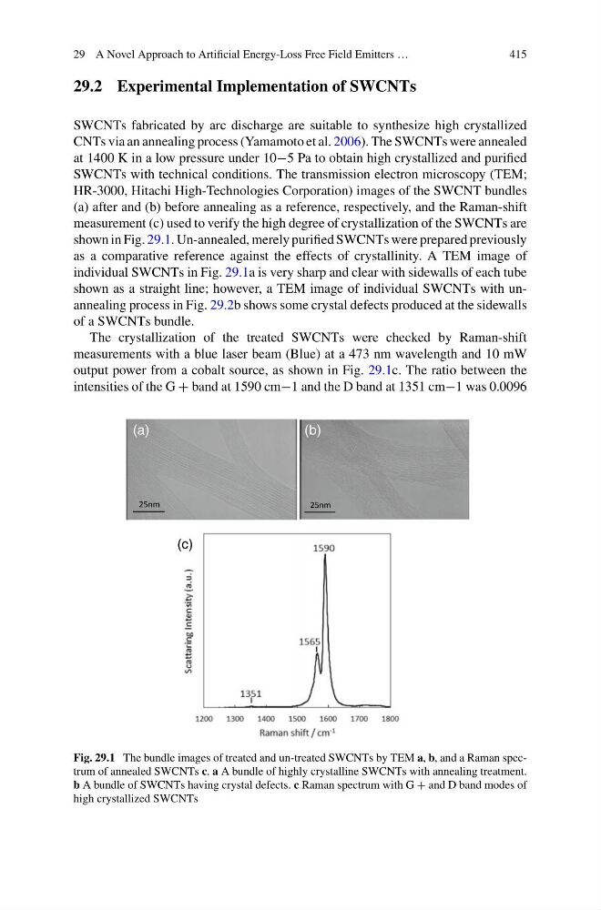
HR-3000, Hitachi High-Technologies Corporation) images of the SWCNT bundles
(a) after and (b) before annealing as a reference, respectively, and the Raman-shift
measurement (c) used to verify the high degree of crystallization of the SWCNTs are
shown in Fig. 29.1. Un-annealed, merely purified SWCNTs were prepared previously
as a comparative reference against the effects of crystallinity. A TEM image of
individual SWCNTs in Fig. 29.1a is very sharp and clear with sidewalls of each tube
shown as a straight line; however, a TEM image of individual SWCNTs with unannealing process in Fig. 29.2b shows some crystal defects produced at the sidewalls
of a SWCNTs bundle.
The crystallization of the treated SWCNTs were checked by Raman-shift
measurements with a blue laser beam (Blue) at a 473 nm wavelength and 10 mW
output power from a cobalt source, as shown in Fig. 29.1c. The ratio between the
intensities of the G + band at 1590 cm−1 and the D band at 1351 cm−1 was 0.0096
25nm
25nm
(a)
(b)
(c)
Fig. 29.1 The bundle images of treated and un-treated SWCNTs by TEM a, b, and a Raman spectrum of annealed SWCNTs c. a A bundle of highly crystalline SWCNTs with annealing treatment.
b A bundle of SWCNTs having crystal defects. c Raman spectrum with G + and D band modes of
high crystallized SWCNTs
415
29.2 Experimental Implementation of SWCNTs
SWCNTs fabricated by arc discharge are suitable to synthesize high crystallized
CNTs via an annealing process (Yamamoto et al. 2006). The SWCNTs were annealed
at 1400 K in a low pressure under 10−5 Pa to obtain high crystallized and purified
SWCNTs with technical conditions. The transmission electron microscopy (TEM;
HR-3000, Hitachi High-Technologies Corporation) images of the SWCNT bundles
(a) after and (b) before annealing as a reference, respectively, and the Raman-shift
measurement (c) used to verify the high degree of crystallization of the SWCNTs are
shown in Fig. 29.1. Un-annealed, merely purified SWCNTs were prepared previously
as a comparative reference against the effects of crystallinity. A TEM image of
individual SWCNTs in Fig. 29.1a is very sharp and clear with sidewalls of each tube
shown as a straight line; however, a TEM image of individual SWCNTs with unannealing process in Fig. 29.2b shows some crystal defects produced at the sidewalls
of a SWCNTs bundle.
The crystallization of the treated SWCNTs were checked by Raman-shift
measurements with a blue laser beam (Blue) at a 473 nm wavelength and 10 mW
output power from a cobalt source, as shown in Fig. 29.1c. The ratio between the
intensities of the G + band at 1590 cm−1 and the D band at 1351 cm−1 was 0.0096
25nm
25nm
(a)
(b)
(c)
Fig. 29.1 The bundle images of treated and un-treated SWCNTs by TEM a, b, and a Raman spectrum of annealed SWCNTs c. a A bundle of highly crystalline SWCNTs with annealing treatment.
b A bundle of SWCNTs having crystal defects. c Raman spectrum with G + and D band modes of
high crystallized SWCNTs