

15 Super-Resolution Imaging and Microscopy by Dielectric …
383
15.2.2 Dielectric Nanoparticle-Based Metamaterial
Superlens
As many studies reveal that most metal-based metamaterials suffer from intrinsic
loss at high optical frequencies, which cause them to be unfavorable in near-infrared
and visible region [95–98]. Moreover, metal-based plasmonic components have low
transmission efficiency at optical frequencies, thus making them less useful for optical waveguiding over long distances or through bulk three-dimensional (3D) structures [99, 100]. Unlike the metal-based metamaterials, dielectric metamaterials use
the near-field coupling between transparent (low absorption), high-refractive index
dielectric building blocks, which perform similar optical phenomena to metallic
nano-resonators, but with much lower energy dissipation [101–104]. Meanwhile,
high transmission and diffraction efficiencies of dielectric components make it possible to move optical metamaterials from current 2D metasurfaces or layered metamaterials to truly 3D metamaterials [99]. New types of particle-lens—metamaterial
solid immersion lens (mSIL)—has recently been proposed and developed by us
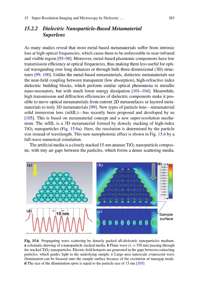
[105]. This is based on metamaterial concept and a new super-resolution mechanism. The mSIL is a 3D metamaterial formed by densely stacking of high-index
TiO 2 nanoparticles (Fig. 15.6a). Here, the resolution is determined by the particle
size instead of wavelength. This new nanophotonic effect is shown in Fig. 15.6 by a
full-wave numerical simulation.
The artificial media is a closely stacked 15-nm anatase TiO 2 nanoparticle composite, with tiny air gaps between the particles, which forms a dense scattering media.
Fig. 15.6 Propagating wave scattering by densely packed all-dielectric nanoparticles medium.
a schematic drawing of a nanoparticle stacked media. b Plane wave (λ = 550 nm) passing through
the stacked TiO 2 nanoparticles. Electric field hotspots are generated in the gaps between contacting
particles, which guides light to the underlying sample. c Large-area nanoscale evanescent wave
illumination can be focused onto the sample surface because of the excitation of nanogap mode.
d The size of the illumination spots is equal to the particle size of 15 nm [105]
383
15.2.2 Dielectric Nanoparticle-Based Metamaterial
Superlens
As many studies reveal that most metal-based metamaterials suffer from intrinsic
loss at high optical frequencies, which cause them to be unfavorable in near-infrared
and visible region [95–98]. Moreover, metal-based plasmonic components have low
transmission efficiency at optical frequencies, thus making them less useful for optical waveguiding over long distances or through bulk three-dimensional (3D) structures [99, 100]. Unlike the metal-based metamaterials, dielectric metamaterials use
the near-field coupling between transparent (low absorption), high-refractive index
dielectric building blocks, which perform similar optical phenomena to metallic
nano-resonators, but with much lower energy dissipation [101–104]. Meanwhile,
high transmission and diffraction efficiencies of dielectric components make it possible to move optical metamaterials from current 2D metasurfaces or layered metamaterials to truly 3D metamaterials [99]. New types of particle-lens—metamaterial
solid immersion lens (mSIL)—has recently been proposed and developed by us
[105]. This is based on metamaterial concept and a new super-resolution mechanism. The mSIL is a 3D metamaterial formed by densely stacking of high-index
TiO 2 nanoparticles (Fig. 15.6a). Here, the resolution is determined by the particle
size instead of wavelength. This new nanophotonic effect is shown in Fig. 15.6 by a
full-wave numerical simulation.
The artificial media is a closely stacked 15-nm anatase TiO 2 nanoparticle composite, with tiny air gaps between the particles, which forms a dense scattering media.
Fig. 15.6 Propagating wave scattering by densely packed all-dielectric nanoparticles medium.
a schematic drawing of a nanoparticle stacked media. b Plane wave (λ = 550 nm) passing through
the stacked TiO 2 nanoparticles. Electric field hotspots are generated in the gaps between contacting
particles, which guides light to the underlying sample. c Large-area nanoscale evanescent wave
illumination can be focused onto the sample surface because of the excitation of nanogap mode.
d The size of the illumination spots is equal to the particle size of 15 nm [105]