

(EELS) [6–8] and energy-dispersive X-ray spectroscopy (EDS). However, these
early results were not readily adopted by the community of biological electron
microscopists. Until recently, biological applications of STEM were not mostly
focused on the cellular context [9], but rather on other applications, such as precise
mass measurements for proteins [10–14], and even demonstrations for sequencing
DNA [15]. Today, STEM is again being explored for imaging and analysis of biological cells, including imaging of wet cells using special vacuum-tight chambers
[16], low-voltage STEM in SEM instruments [17], and chemical composition [18,
19]. In particular, STEM imaging is increasingly appreciated as an important method
for obtaining tomograms of thick biological specimens whether they are fixed,
embedded sections, or cryo-preserved vitrified samples.
The advantages lie with the method of STEM imaging, where the electron beam
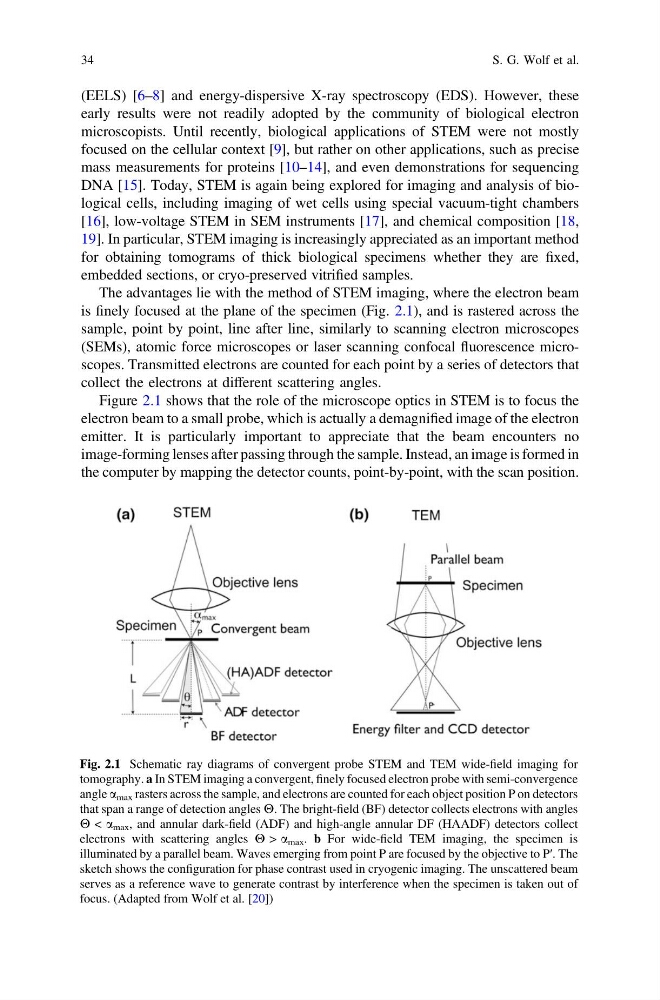
is finely focused at the plane of the specimen (Fig. 2.1), and is rastered across the
sample, point by point, line after line, similarly to scanning electron microscopes
(SEMs), atomic force microscopes or laser scanning confocal fluorescence microscopes. Transmitted electrons are counted for each point by a series of detectors that
collect the electrons at different scattering angles.
Figure 2.1 shows that the role of the microscope optics in STEM is to focus the
electron beam to a small probe, which is actually a demagnified image of the electron
emitter. It is particularly important to appreciate that the beam encounters no
image-forming lenses after passing through the sample. Instead, an image is formed in
the computer by mapping the detector counts, point-by-point, with the scan position.
Fig. 2.1 Schematic ray diagrams of convergent probe STEM and TEM wide-field imaging for
tomography. a In STEM imaging a convergent, finely focused electron probe with semi-convergence
angle a max rasters across the sample, and electrons are counted for each object position P on detectors
that span a range of detection angles H. The bright-field (BF) detector collects electrons with angles
H < a max , and annular dark-field (ADF) and high-angle annular DF (HAADF) detectors collect
electrons with scattering angles H > a max . b For wide-field TEM imaging, the specimen is
illuminated by a parallel beam. Waves emerging from point P are focused by the objective to P′. The
sketch shows the configuration for phase contrast used in cryogenic imaging. The unscattered beam
serves as a reference wave to generate contrast by interference when the specimen is taken out of
focus. (Adapted from Wolf et al. [20])
34
S. G. Wolf et al.
early results were not readily adopted by the community of biological electron
microscopists. Until recently, biological applications of STEM were not mostly
focused on the cellular context [9], but rather on other applications, such as precise
mass measurements for proteins [10–14], and even demonstrations for sequencing
DNA [15]. Today, STEM is again being explored for imaging and analysis of biological cells, including imaging of wet cells using special vacuum-tight chambers
[16], low-voltage STEM in SEM instruments [17], and chemical composition [18,
19]. In particular, STEM imaging is increasingly appreciated as an important method
for obtaining tomograms of thick biological specimens whether they are fixed,
embedded sections, or cryo-preserved vitrified samples.
The advantages lie with the method of STEM imaging, where the electron beam
is finely focused at the plane of the specimen (Fig. 2.1), and is rastered across the
sample, point by point, line after line, similarly to scanning electron microscopes
(SEMs), atomic force microscopes or laser scanning confocal fluorescence microscopes. Transmitted electrons are counted for each point by a series of detectors that
collect the electrons at different scattering angles.
Figure 2.1 shows that the role of the microscope optics in STEM is to focus the
electron beam to a small probe, which is actually a demagnified image of the electron
emitter. It is particularly important to appreciate that the beam encounters no
image-forming lenses after passing through the sample. Instead, an image is formed in
the computer by mapping the detector counts, point-by-point, with the scan position.
Fig. 2.1 Schematic ray diagrams of convergent probe STEM and TEM wide-field imaging for
tomography. a In STEM imaging a convergent, finely focused electron probe with semi-convergence
angle a max rasters across the sample, and electrons are counted for each object position P on detectors
that span a range of detection angles H. The bright-field (BF) detector collects electrons with angles
H < a max , and annular dark-field (ADF) and high-angle annular DF (HAADF) detectors collect
electrons with scattering angles H > a max . b For wide-field TEM imaging, the specimen is
illuminated by a parallel beam. Waves emerging from point P are focused by the objective to P′. The
sketch shows the configuration for phase contrast used in cryogenic imaging. The unscattered beam
serves as a reference wave to generate contrast by interference when the specimen is taken out of
focus. (Adapted from Wolf et al. [20])
34
S. G. Wolf et al.